Key Takeaways for Automated ICT Selection
-
Bed-of-nails ICT supports high-volume production with fast parallel testing but requires custom fixtures and stable designs.
-
Flying probe testers support prototypes and low-volume runs without fixtures, though test cycles slow throughput at higher volumes.
-
Hybrid systems combine bed-of-nails speed with flying probe access to cover complex, high-density PCBAs.
-
Boundary scan uses embedded IC circuitry to test inaccessible BGA and multi-layer interconnects.
-
Pro-Active Engineering provides integrated ICT solutions from prototype to production with ISO, AS9100 and ITAR certifications; discuss testing requirements to identify risk mitigation strategies.
Core Automated ICT Methods for Complex PCBAs
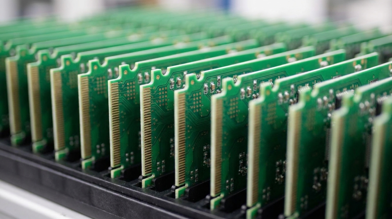
Bed-of-nails ICT systems use fixed arrays of spring-loaded probes that contact multiple test points simultaneously, a parallel testing approach that suits high-volume production where throughput matters. This simultaneous contact enables broad coverage of power rails, digital signals and analog circuits across dense PCBAs in a single test cycle.
Where bed-of-nails focuses on speed, flying probe testers prioritize flexibility. Flying probe systems employ movable probes controlled by precision motors that contact test points sequentially. This approach suits prototypes and low-volume production where fast program changes and minimal tooling costs matter.
Hybrid ICT systems combine bed-of-nails and flying probe technologies in one platform to balance speed and access. These systems use fixed probes for dense test point arrays that justify fixture investment. Flying probes then reach difficult locations or support design variations without fixture changes, which preserves coverage as layouts evolve.
Boundary scan testing uses embedded test circuitry within ICs to reach internal nodes and interconnects that probes cannot touch. IEEE 1149.1 boundary scan incorporates TAP controllers and serial data paths. This structure enables test access for complex chips and AI accelerators where physical probe access proves impossible.
Each method addresses specific PCBA testing needs. Bed-of-nails systems deliver speed and repeatability for stable, high-volume designs. Flying probe testers support evolving prototypes and high-mix low-volume work. Boundary scan covers inaccessible interconnects in high-density packages, while hybrid systems blend these strengths on a single platform.
Head-to-Head ICT Comparison for High-Density PCBAs
Throughput, Cost and Flexibility: Bed-of-Nails vs Flying Probe
Throughput differences between bed-of-nails and flying probe systems become clear in production environments. Bed-of-nails ICT fixtures enable fast automated testing per board because many points are measured in one cycle. Flying probe testers take longer because sequential probing extends test time, which limits capacity at scale. In production lines that run thousands of boards each month, bed-of-nails systems deliver cycle time advantages that directly affect manufacturing output.
Cost structures shift with volume and design maturity. Flying probe testers eliminate fixture costs and rely on software configuration for setup. This model fits early prototypes and small batches. Bed-of-nails ICT requires custom fixtures, and fixture costs and build times depend on test point count and mechanical complexity. At higher volumes, lower per-board test cost from bed-of-nails offsets the initial fixture investment, while flying probe testing becomes more expensive per unit.
Setup flexibility shapes prototype and new product introduction phases. Flying probe testers support program changes through software reconfiguration, which supports prototypes, pilot runs and high-mix low-volume production. Bed-of-nails systems require fixture modifications when designs change, so they align better with stable layouts and established products.
Hybrids and Boundary Scan for BGA and 3D Packages
High-density BGAs and multi-layer boards create accessibility challenges that traditional probe-based testing cannot fully address. In chiplet package designs and 3D integration, boundary scan cells enable testing of through-silicon vias and interconnect chains after assembly, addressing inaccessible pins in multi-die environments. This capability supports complex computing and AI accelerator PCBAs where direct probe access is physically blocked.
Hybrid ICT systems respond to these constraints by combining parallel and sequential testing methods on one platform. These systems use bed-of-nails arrays for accessible test points and power distribution networks. Flying probes then handle edge connectors, fine-pitch components and regions where fixture complexity or mechanical stress would be prohibitive. This combination delivers coverage that adapts to varying board densities and access limits.
Pro-Active Engineering applies this multi-technology strategy through integrated flying probe, in-circuit and functional testing systems that work together to validate complex aerospace and defense PCBAs. This coordinated approach supports comprehensive fault detection across prototype and production phases and maintains the traceability and documentation required for regulated programs.
Decision Framework for Matching ICT to PCBA Requirements
Volume requirements provide the first filter for automated ICT selection. Bed-of-nails fixtures suit production runs where fixture costs spread across many units. Flying probe systems align with prototype phases and low-volume production where rapid setup and design agility matter more than cycle time.
Board complexity and access needs refine the choice beyond volume. Dense BGAs, fine-pitch components and multi-layer constructions often require boundary scan or hybrid approaches to maintain coverage. ICT test fixtures catch defects before functional testing, which reduces rework and protects downstream processes.
Design stability further shapes fixture-based decisions. Frequent layout changes favor flying probe systems that adapt through software updates. Stable production designs benefit from bed-of-nails systems that deliver high-speed testing and consistent coverage once fixtures are in place.
Partnership with Pro-Active Engineering aligns automated testing with design and manufacturing workflows under one provider. This integrated model reduces risks from vendor fragmentation and supports smooth transitions from prototype validation to production testing. Connect with Pro-Active Engineering to match volume, complexity and compliance requirements with the right ICT approach.
Pro-Active Engineering ICT in Action for Complex Programs
Pro-Active Engineering links rapid prototyping with scalable production testing through a unified test strategy. Flying probe systems support prototype validation and allow design iterations without fixture delays, which accelerates early learning cycles. Bed-of-nails ICT systems then provide throughput and repeatability for production volumes while preserving test intent established during development.
Aerospace and defense applications gain from this comprehensive testing integration. Advanced interconnects and high-density packages require specialized combinations of ICT, boundary scan and functional testing. These coordinated methods help assemblies meet reliability expectations for mission-critical use while maintaining consistent documentation.
US-based manufacturing with ITAR compliance addresses security and supply chain concerns for sensitive programs. Certified quality management systems support traceability and documentation across design, test and production. This structure reduces compliance gaps that can delay approvals or trigger audit findings.
The integrated workflow also closes prototype-to-production gaps. Design for manufacturability insights inform prototype testing strategies. Production testing then builds on development validation, which maintains consistent coverage as builds scale.
Risks, Limitations and Practical Evaluation Checklist
Bed-of-nails systems require upfront fixture investment and design stability to deliver value. Fixture costs depend on test point count and complexity. Design changes after fixture completion introduce additional cost and schedule impact because fixtures must be revised or rebuilt.
Flying probe systems introduce throughput limits in high-volume production. Sequential probing slows test speeds at high volumes, which can constrain capacity. Probe wear and calibration also create maintenance needs that require planning and periodic downtime.
Evaluation criteria should cover test coverage, volume projections, design stability, access constraints and workflow integration. Consider boundary scan for inaccessible interconnects, AOI and X-ray integration for structural defects, and compliance documentation for regulated markets.
Frequently Asked Questions
Key Differences Between ICT and Flying Probe Testing
ICT systems use fixed bed-of-nails fixtures where multiple probes contact test points simultaneously, which suits high-volume production. Flying probe testers use movable probes that contact test points sequentially and support prototypes and design changes without fixture modifications. Selection depends on volume targets, design stability and acceptable setup time.
ICT Approaches for High-Density Boards
High-density boards benefit from hybrid strategies that combine several testing technologies. Flying probe systems reach fine-pitch components and edge connectors, while boundary scan covers inaccessible BGA interconnects and internal routing. Bed-of-nails systems provide broad coverage for accessible test points at production volumes. The most effective plan integrates these methods based on specific density and access conditions.
Benefits of Hybrid ICT Systems
Hybrid ICT systems combine the speed of bed-of-nails testing with the flexibility of flying probe access to cover varied board densities and access limits. These platforms use fixed probes for dense test point arrays and movable probes for difficult locations, which avoids a forced tradeoff between speed and coverage. Hybrid strategies support complex boards with mixed accessibility requirements across product phases.
Automated Testing Within PCBA Manufacturing
Integrated manufacturing workflows connect automated testing with design, assembly and quality control under a single management system. This structure aligns test strategies with design for manufacturability principles, so prototype testing validates both design and process. Production testing then extends development validation, which reduces vendor handoffs that create communication gaps and quality risks and supports consistent coverage from prototypes through production.
Pro-Active Lead Times and Scaling for ICT Testing
Pro-Active Engineering Speed Shop delivers prototype testing with short lead times using production-grade processes. This model supports design validation without reducing test quality. Test coverage then transitions to bed-of-nails ICT systems for production throughput, which removes prototype-to-production disconnects. The approach maintains quality standards and documentation, while US-based operations support secure supply chain management for defense and aerospace programs.
Conclusion: Integrated ICT Support for Complex PCBAs
Complex PCBAs require testing that balances coverage, throughput and flexibility across development and production phases. Pro-Active Engineering automated testing capabilities validate high-density boards and scale from early development through full manufacturing. Engage with Pro-Active Engineering to structure ICT workflows that reduce program risk and support long-term product reliability.