Last updated: April 17, 2026
Key Takeaways for Bed of Nails ICT
- Bed of nails ICT uses custom pogo-pin fixtures for parallel testing of hundreds of PCB points, detecting shorts, opens, and component values in seconds.
- The five-step process covers fixture design, PCB alignment, pneumatic actuation, signal measurement, and automated fault analysis against golden board baselines.
- Advantages include high throughput and coverage for high-volume production, while limitations include high fixture costs and limited flexibility for design changes.
- Bed of nails works best for stable, high-volume builds, while flying probe offers greater flexibility for prototypes and low-volume runs.
- Pro-Active Engineering provides ISO 9001:2015, AS9100, ITAR-compliant in-house ICT fixtures and testing for zero-defect mission-critical PCBs; get a quote for certified ICT services today.
How Bed of Nails Testing Supports Reliable PCBA Production
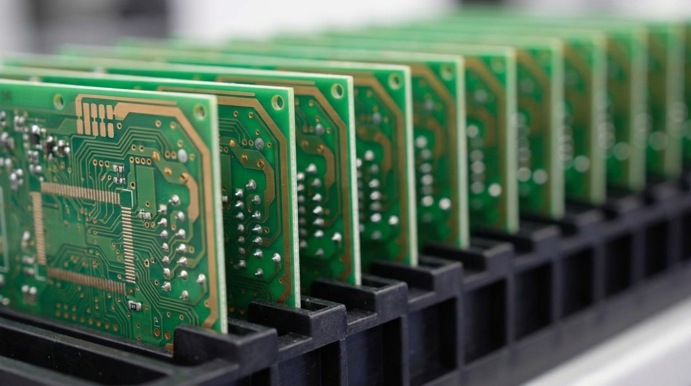
Bed of nails in-circuit testing (ICT) uses a custom fixture with spring-loaded pogo pins arranged like a “bed of nails” to make simultaneous electrical contact with hundreds of test points on a PCB under test (UUT). Powered probes apply signals to verify components, connections, and functionality without powering the full board. This testing method originated in the 1960s as PCB complexity increased, and it has evolved into sophisticated systems that verify shorts, opens, and passive component values with precision. Modern bed of nails testing supports high-reliability PCBA manufacturing, and Pro-Active Engineering applies ICT across production assemblies to protect mission-critical performance.
How Does Bed of Nails In-Circuit Testing Work? Step-by-Step
The bed of nails in-circuit testing process follows five clear steps that together deliver accurate component and net verification.
1. Fixture Design and Fabrication: Engineers create CAD files with probe alignment within 0.1 mm tolerance and DFM considerations for pads greater than 0.8–1 mm diameter. The fixture uses a 100 mil grid pattern that matches common test point layouts.
2. PCB Alignment: The PCB aligns using tooling holes held to ±0.05 mm tolerances or edge clamps. This alignment keeps test points positioned accurately over the probe array.
3. Pneumatic Actuation: Pneumatic or mechanical actuators drive the pin array upward to contact test points, with spring-loaded pins providing 1–2 mm travel strokes. This travel compensates for board warpage and maintains consistent contact force.
4. Signal Application and Measurement: The tester injects DC voltages, currents, or AC signals into the PCB to measure continuity, resistance, capacitance, inductance, and diode orientations across nets and components. These measurements confirm correct component values and connectivity.
5. Fault Analysis: Guardian circuits protect against overvoltage while software sequences node-by-node tests and compares measurements against baselines from a golden board. The system flags deviations as potential defects for repair or rework.
Pro-Active Engineering designs and manufactures custom bed of nails test fixtures in-house, aligning fixture design with PCBA manufacturing processes and shortening time-to-market for complex assemblies.
Inside a Bed of Nails Test Fixture
Understanding the five-step testing process highlights why fixture construction directly affects test reliability and coverage. The fixture controls which test points are reachable, how stable each contact remains, and which defects the system can detect.
A bed of nails test fixture uses several precision-engineered components that work together to create reliable electrical contact. The baseplate holds an array of spring-loaded pogo pins. Receptacles mounted in the probe plate hold spring-loaded probes and provide electrical connections to the signal interface through solder or wire-wrap terminations.
The fixture design often includes feedthrough plates that allow conductors to pass directly through the probe plate, creating short, direct signal paths from probes to the interface for improved signal integrity. For larger fixtures, TPCB (test point carrier board) signal interfaces route signals from probe receptacles to organized connectors on a dedicated PCB, which reduces wiring errors and further improves signal integrity.
Typical bed of nails test fixture costs range from $5,000 to $50,000 depending on complexity, and some vendors deliver development-grade bed-of-nails test fixtures in 2–3 weeks. Pro-Active Engineering’s custom fixture capabilities also support integration with flying probe systems, which extends coverage to both accessible and hard-to-reach test points.
Advantages and Limitations of Bed of Nails PCB Testing
Advantages:
- High throughput with test completion in 5–15 seconds per board
- Test coverage exceeding 90% of nets when properly designed
- Cost-effective for high-volume production after fixture amortization
- Simultaneous testing of multiple points reduces overall test time and supports tight production schedules.
Limitations:
- High initial fixture costs make bed of nails unsuitable for many low-volume or rapidly changing designs.
- Limited flexibility for design changes once the fixture is manufactured, which can require rework or a new fixture.
- Inability to access BGA solder balls or QFN/DFN thermal pads located underneath packages after assembly
- Fixture development often requires multiple weeks depending on vendor and requirements
Design for Manufacturability (DFM) Best Practices: SMD test pads should have a preferred diameter greater than 1.0 mm or minimum 0.8 mm for reliable contact with standard spring-loaded crown-tip probes. Planning test points early in the design phase increases coverage and keeps fixture complexity manageable.
Bed of Nails vs Flying Probe: Key Differences
The choice between bed of nails and flying probe testing depends mainly on production volume, design stability, and budget for fixtures. The comparison below shows how each method aligns with different manufacturing scenarios.
| Testing Method | Test Speed | Initial Cost | Flexibility | Best Volume |
|---|---|---|---|---|
| Bed of Nails | 5–15 seconds per board | High fixture cost, low per-unit cost | Low (fixed probe layout) | High volume |
| Flying Probe | Slower due to sequential contact | Low fixture cost, higher per-unit cost | High (programmable probes) | Low to medium volume |
Pro-Active Engineering offers both bed of nails and flying probe testing through our Speed Shop rapid prototyping service, which supports tailored test strategies based on volume requirements and design constraints. Get a quote to determine the most cost-effective testing approach for your specific application.
Real-World Bed of Nails Use Cases and 2026 Best Practices
Aerospace and medical device manufacturers rely on bed of nails electronic testing for vibration-tested boards and high-reliability assemblies where single-point failures can have severe consequences. These demanding environments increase the need for stable probe contact and consistent measurements across many cycles. Probe wear and false calls become common challenges under these conditions, so manufacturers pair ICT with integrated AOI inspection and Nadcap-accredited processes to validate both equipment performance and test results.
2026 industry trends reflect two converging pressures on bed of nails testing. First, AI-driven test optimization algorithms reduce false positives by learning to separate genuine defects from measurement noise. Second, CMMC and NIST compliance requirements increase demand for domestic testing capabilities as defense contractors document secure supply chains. These combined demands for higher accuracy and secure, local sourcing push modern bed of nails test jig designs toward advanced materials and precision manufacturing that improve repeatability and reduce maintenance.
Pro-Active Engineering applies 100% inspection protocols that combine bed of nails ICT with AOI and functional testing to support zero-defect delivery for mission-critical applications. Our integrated approach consistently reduces defects compared to fragmented testing flows and helps customers maintain quality targets as volumes scale.
Why Choose Pro-Active Engineering for Bed of Nails Electronic Testing
Pro-Active Engineering serves as a U.S.-based partner for integrated bed of nails testing and PCBA manufacturing. Our end-to-end workflow delivers 2–5 day prototypes through the Speed Shop, comprehensive ICT and functional testing, and complete box build capabilities in a single facility. With 30+ years of experience, 45,000 square feet of manufacturing space, and 25 employees in Engineering & Technical departments, we support complex, mission-critical electronics programs.
Our certifications include ISO 9001:2015, AS9100, ITAR registration, JCP certification, and Nadcap accreditation, which together confirm compliance with stringent aerospace, defense, and medical requirements. A recent aerospace customer achieved 30% defect reduction and faster time-to-market through our integrated design-to-test workflow, demonstrating the impact of coordinated fixture design, ICT, and manufacturing.
Ready to experience the Pro-Active Engineering advantage? Request a quote for custom ICT fixtures and testing tailored to your mission-critical requirements.
Frequently Asked Questions
What is a bed of nails test jig?
A bed of nails test jig is a custom fixture that contains an array of spring-loaded pogo pins arranged to match specific test points on a PCB. The jig provides mechanical support and electrical connections so automated testing equipment can verify component values, detect shorts and opens, and confirm assembly quality. Typical fixtures include precision alignment mechanisms, pneumatic actuation systems, and interface electronics that connect to automated test equipment.
What does a bed of nails test fixture cost?
Bed of nails test fixture costs vary based on PCB complexity, number of test points, and required precision, and they represent a significant upfront investment that is spread across high-volume production runs. While initial costs are high, the per-unit testing cost becomes very low at scale, which makes bed of nails attractive once volumes justify the fixture. Pro-Active Engineering provides detailed cost analysis, ROI projections, and volume breakeven estimates for each custom fixture project.
What are the key differences between bed of nails vs flying probe testing?
Bed of nails testing uses fixed probe arrays for simultaneous contact with all test points, which supports very short test cycles suited to high-volume production. Flying probe testing uses movable probes that contact points sequentially, which offers greater flexibility for prototypes and frequent design changes but increases test time. Bed of nails requires higher initial fixture investment and delivers lower per-unit costs, while flying probe keeps setup costs low but maintains higher per-unit testing expenses.
Can Pro-Active Engineering build custom bed of nails fixtures?
Yes. Pro-Active Engineering designs and manufactures custom bed of nails fixtures in-house as part of our integrated PCBA testing services. Our engineering team collaborates with customers to refine fixture design for strong test coverage, applying DFM principles from the initial PCB layout phase. We handle complete fixture development, including CAD design, precision machining, probe selection, and integration with automated test equipment for smooth production rollout.
What is bed of nails testing used for in electronics manufacturing?
Bed of nails testing verifies electrical connectivity, component values, and assembly quality in electronics manufacturing. The method detects shorts, opens, missing components, incorrect component values, and polarity errors through targeted electrical measurements. It proves especially valuable for high-volume production of mission-critical electronics in aerospace, defense, and medical device applications where thorough verification supports reliability and regulatory compliance.
Conclusion
Bed of nails in-circuit testing delivers high throughput and broad coverage for high-volume PCB production while keeping per-unit test costs low once fixtures are in place. The structured process from fixture design through fault analysis supports reliable verification of mission-critical assemblies. Contact Pro-Active Engineering today for integrated ICT solutions that combine custom fixture design, rapid prototyping, and certified manufacturing in one coordinated workflow.