Last updated: April 17, 2026
Key Takeaways for Complex PCB ICT Decisions
- ALLPCB’s bed-of-nails ICT struggles with BGA access, dense layouts, and fine-pitch components in complex PCBs, which increases the risk of test escapes in mission-critical applications.
- Pro-Active Engineering’s flying probe testing reaches all accessible test points without custom fixtures and delivers high fault coverage for high-density assemblies.
- Pro-Active delivers 2-5 day prototype testing with full production processes, ITAR compliance, and certifications like AS9100 and Nadcap, while ALLPCB requires 2-4 weeks for fixture development.
- Pro-Active’s integrated workflow combines AOI, ICT, functional, and environmental tests with full traceability to support aerospace, defense, and medical reliability requirements.
- Choose Pro-Active Engineering for zero-failure complex PCB testing and get a custom testing quote for your next complex assembly from a US-based partner.
How ALLPCB Approaches ICT and PCB Validation
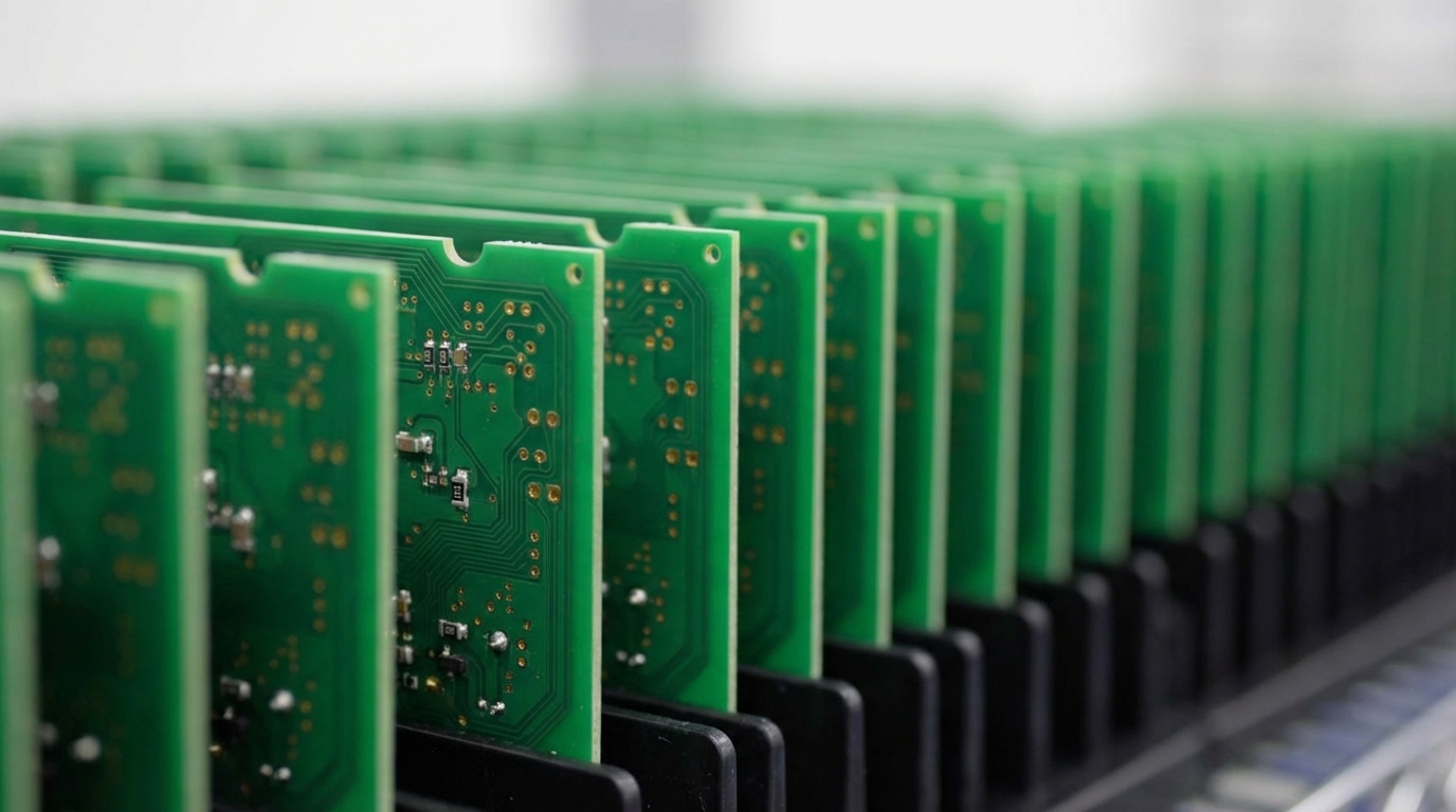
ALLPCB’s in-circuit testing capabilities center on three primary approaches for PCB validation, each suited to different production volumes and board complexities.
1. Bed-of-nails ICT systems that automatically test electrical parameters such as resistance down to 0.1 ohms and capacitance within 1% tolerance, designed for high-volume production environments.
2. Flying probe testing offered as an alternative for prototypes and small batches, though it is slower than ICT for production volumes.
3. Integrated AOI systems that measure solder paste height, volume, and alignment for high-density boards and detect component offsets as small as 0.1 mm.
ALLPCB’s bed-of-nails fixtures deliver fast, cost-effective testing for simple boards, often completing tests in 5-15 seconds per unit. Their systems support impedance values in the range of 1 to 100 ohms for typical PCB traces and signal speeds exceeding 1 GHz in high-speed designs. These strengths diminish when boards become more complex and high density.
Key ALLPCB ICT Limitations for High-Density & Multi-Layer Boards
These constraints become critical failures in high-density and multi-layer designs. ALLPCB’s bed-of-nails ICT approach encounters several limitations that make it unsuitable for many complex assemblies.
- BGA under-ball access issues: Traditional bed-of-nails in-circuit testers are structurally inadequate for high-density PCB assemblies due to severe accessibility constraints from fixed test fixtures.
- Limited coverage in dense layouts: Bed-of-nails ICT coverage suffers in ultra-dense PCB layouts without additional vias, which restricts access to inner nets.
- High fixture costs and delays: High fixture costs and schedule impact arise because custom fixtures require the 2-4 week development cycle mentioned earlier.
- Overseas logistics and ITAR non-compliance: Extended lead times, export controls, and security risks complicate regulated aerospace and defense programs.
- Low-volume scalability challenges: ALLPCB bed-of-nails high initial custom fixture costs amortize over thousands of units, which makes prototyping and low-volume runs economically impractical.
The following table summarizes how each limitation translates into concrete operational risks.
| Testing Aspect | ALLPCB Bed-of-Nails | Limitation Impact |
|---|---|---|
| BGA Access | Structurally inadequate | Critical nets untested |
| Dense Layout Coverage | Suffers without additional vias | Reduced fault detection |
| Fixture Development | 2-4 weeks | Program delays |
| Fine-Pitch Components | Limited probe access | Test escapes |
These limitations, from untested critical nets to schedule slips, create substantial risks in mission-critical applications where aerospace applications contribute to global in-circuit test market demand, driven by strict reliability requirements. See how Pro-Active eliminates these risks by contacting our US-based testing team.
Why Pro-Active Engineering Excels in ICT for Complex PCB Assemblies
Pro-Active Engineering resolves these limitations with an integrated testing approach that combines flying probe technology and comprehensive quality control systems. Their flying probe testing provides high fault coverage by detecting opens, shorts, missing components, incorrect component orientation, solder bridges, resistance issues, capacitance anomalies, and diode polarity errors without requiring custom bed-of-nails fixtures.
Key advantages build on each other to support complex, regulated programs.
- Superior access capabilities: Flying probe testers enable flexible access to all test points with pinpoint accuracy, which removes BGA accessibility constraints.
- Rapid prototype testing: Speed Shop delivers production-ready prototypes in 2-5 days using full production processes, which accelerates design validation.
- Comprehensive quality integration: 100% AOI, flying probe, in-circuit, and functional testing run in a single coordinated workflow for consistent coverage.
- ITAR compliance and certifications: ISO 9001:2015, AS9100, ITAR registration, JCP certification, and Nadcap accreditation support demanding regulatory requirements.
- Advanced traceability: Full documentation control and component traceability support audits and field investigations for mission-critical applications.
- Thermal and vibration testing: Specialized environmental testing validates performance in harsh operating conditions.
Pro-Active’s DFM integration reduces redesign cycles by catching manufacturability issues early in development. Their 30+ years of experience in complex electronics manufacturing, combined with advanced interconnect capabilities such as wire bonding and flip chip assembly, position them as a strong choice for regulated industries that require zero-failure reliability.
ALLPCB vs Pro-Active: ICT Comparison Table for Complex PCBs
The following comparison demonstrates Pro-Active’s advantages across every critical dimension of complex PCB testing.
| Feature | ALLPCB | Pro-Active Engineering | Winner |
|---|---|---|---|
| BGA Access | Structurally inadequate | Flexible access to all test points | Pro-Active |
| Test Coverage | Suffers in ultra-dense layouts | High fault coverage | Pro-Active |
| Prototype Lead Time | 2-4 weeks fixture development | 2-5 days Speed Shop | Pro-Active |
| ITAR Compliance | Overseas, non-compliant | ITAR registered, US-based | Pro-Active |
| Low-Volume Economics | Requires thousands of units to amortize | 1-piece MOQ capability | Pro-Active |
| Integration | ICT only | ICT + AOI + functional + thermal | Pro-Active |
| Certifications | Limited | ISO 9001:2015, AS9100, Nadcap | Pro-Active |
This comparison highlights Pro-Active Engineering’s advantages for complex PCB testing in regulated industries where defense and government services represent a significant portion of the global ICT market, reflecting the need for high-stability electronics.
Best ICT Practices for Aerospace and Defense PCBs
Mission-critical applications benefit from testing strategies that combine multiple methodologies instead of relying on traditional ICT alone. Medical electronics account for a significant share of the ICT market, essential for validating circuits in patient monitoring and life-support systems under stringent regulatory standards, which underscores the value of comprehensive testing approaches.
When evaluating providers for such multi-methodology approaches, prioritize these criteria that directly impact mission-critical reliability.
- Test coverage percentage for critical nets
- ITAR compliance and security protocols
- Integration with functional and environmental testing
- Prototype-to-production scalability
- Documentation and traceability capabilities
ALLPCB may support simple prototype validation, but Pro-Active Engineering’s integrated approach becomes essential for complex, high-reliability assemblies. Start your 2-5 day prototype with a quick consultation.
Frequently Asked Questions
Does ALLPCB offer flying probe testing for BGA components?
ALLPCB offers flying probe testing as an alternative to bed-of-nails ICT, but their capabilities remain limited for complex BGA assemblies. Their flying probe systems focus on prototypes and small batches rather than comprehensive BGA under-ball testing. Pro-Active Engineering’s flying probe technology specifically addresses BGA accessibility challenges with advanced probe positioning and comprehensive test coverage for high-density interconnects.
What are Pro-Active Engineering’s ICT lead times compared to ALLPCB?
Pro-Active Engineering delivers prototype testing through their Speed Shop in 2-5 days, while ALLPCB’s bed-of-nails approach often requires 4-8 weeks for fixture development and test program creation. This difference results from Pro-Active’s flying probe technology, which removes custom fixture requirements and enables immediate testing of new designs with rapid iteration cycles for complex PCB development.
What ITAR-compliant alternatives exist to ALLPCB for defense applications?
Pro-Active Engineering provides a fully ITAR-compliant alternative with comprehensive certifications including ISO 9001:2015, AS9100, JCP certification, and Nadcap accreditation. Their Wisconsin-based facility supports domestic manufacturing with secure processes, controlled documentation, and full traceability required for defense and aerospace programs. This approach removes the security risks and logistics complications associated with overseas testing services.
How do complex PCB ICT costs compare between ALLPCB and Pro-Active?
ALLPCB may offer lower per-unit testing costs, but Pro-Active Engineering delivers better total cost of ownership through reduced redesign cycles, eliminated fixture costs, faster time-to-market, and integrated DFM feedback. Their approach prevents costly late-stage discoveries and rework that frequently occur with traditional bed-of-nails testing of complex assemblies, particularly in regulated industries where failure costs are substantial.
What are the key differences between bed-of-nails and flying probe ICT methods?
Bed-of-nails ICT uses fixed test fixtures with predetermined probe locations, which makes it fast for high-volume production but inflexible for design changes and limited in accessing dense layouts. Flying probe ICT uses movable probes that can access any exposed copper or test point, which provides greater flexibility and coverage for complex assemblies. Flying probe technology excels in prototype testing, low-volume production, and high-density designs where traditional fixtures cannot provide adequate access.
Conclusion: Choosing the Right ICT Partner for Complex PCBs
ALLPCB’s bed-of-nails ICT approach faces fundamental limitations when testing complex PCB assemblies, especially in high-density designs with BGA components and fine-pitch interconnects. Pro-Active Engineering’s integrated flying probe testing, combined with comprehensive quality control and ITAR compliance, offers a robust path for regulated industries that require zero-failure reliability. Their track record in aerospace, defense, and medical electronics, supported by advanced certifications and rapid prototyping capabilities, establishes them as a strong US-based alternative for mission-critical PCB testing. Discuss your testing requirements with Pro-Active’s certified engineers.