Last updated: April 17, 2026
Key Takeaways
- Run thermal simulations early with CFD tools to predict hotspots and avoid costly prototype spins.
- Use thermal via arrays, heavy copper pours, and smart component zoning to spread heat and support airflow.
- Select high-Tg metal-core materials and advanced attachment methods like silver sintering to move heat efficiently.
- Integrate heatsinks, TIMs, and DFM reviews so designs build reliably and hit first-pass thermal targets.
- Partner with Pro-Active Engineering for ITAR-compliant, rapid prototyping with proven thermal management support.
Design Context for High-Power Thermal Management
This guide focuses on lead design engineers building high-power PCB prototypes with power densities above 0.5-1.0 W/cm². Key concepts include thermal vias that move heat vertically, heavy copper with ≥3 oz/ft² thickness, coefficient of thermal expansion (CTE) mismatch between materials, thermal interface materials (TIMs), computational fluid dynamics (CFD) simulation, and design for manufacturability (DFM).
Current projects often require ITAR-compliant onshoring and rapid prototype cycles that still match production quality. Advanced techniques such as silver sintering and direct thermal path technology now support many high-reliability designs. Get a Speed Shop quote to align your next prototype with these capabilities.
12 Best Practices for PCB Thermal Management in High-Power Prototypes
1. Run Early CFD Simulations to Predict Hotspots
Start thermal simulation with tools like Altium Designer 2026 or ANSYS Icepak before physical layout to reveal hotspots and confirm thermal paths. Beginning this work early reduces expensive prototype iterations because CFD can model realistic power dissipation, airflow, and material properties before you commit to copper. Use actual component power ratings and expected ambient conditions so simulations set baseline thermal targets that you can check against hardware.
2. Zone Component Placement to Support Airflow
Plan component placement around thermal zones that support natural convection and forced airflow. Place high-power ICs away from board edges and enclosure walls where heat can trap and recirculate. Group components with similar power levels and keep heat-sensitive analog circuits separate from power stages. This zoning approach improves heat spreading and limits unwanted thermal coupling between nearby parts.
3. Deploy Thermal Via Arrays per IPC-2221
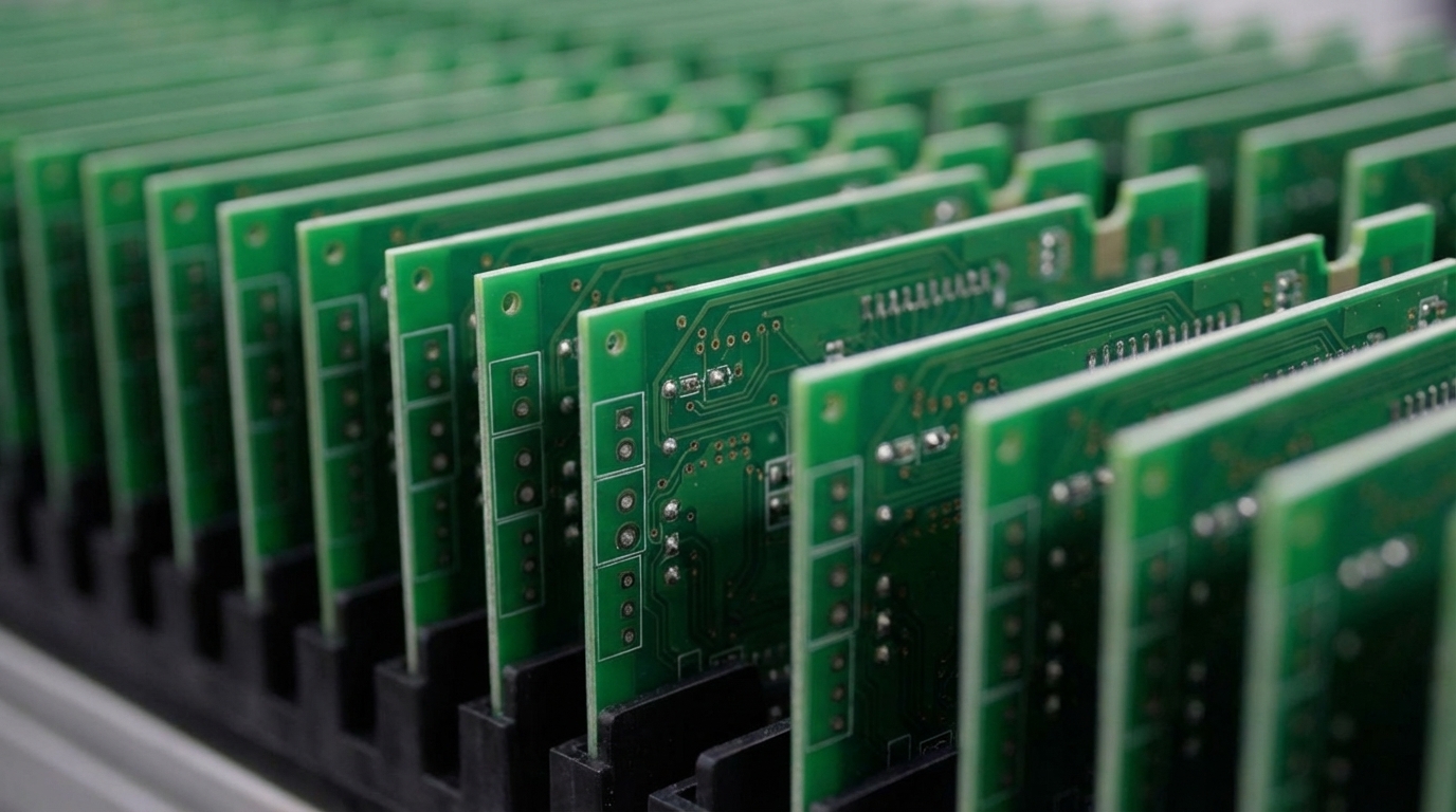
Place dense thermal via arrays directly under exposed thermal pads using 0.3-0.5mm diameter vias with 1mm pitch spacing to move heat into inner layers. Standard 0.3mm vias with 1 oz copper plating can carry about 1.5A of current within safe temperature limits, which supports both thermal and electrical needs. Fill or cap these vias to prevent solder wicking during assembly and to improve thermal conduction. Tie the via arrays directly into large internal copper planes so the board can spread heat efficiently.
4. Widen Power Traces and Use Heavy Copper Pours
Size traces with IPC-2152 calculations and use ≥3 oz/ft² copper thickness on high-current paths. Thicker copper increases current capacity without extreme trace widening, which keeps temperatures within IPC-2152 limits. Heavy copper also spreads heat more effectively and reduces voltage drop across power distribution networks. Get pricing on heavy copper prototypes to support these layouts.
5. Select High-Tg Laminates and Metal-Core Substrates
Choose laminates with glass transition temperatures at or above 170°C, then evaluate metal-core PCBs for demanding thermal loads. Aluminum cores reach 150-235 W/m·K while copper cores reach 380-400 W/m·K, compared to standard FR-4 at about 0.3 W/m·K. Match CTE values between the substrate and key components to reduce solder joint stress during thermal cycling. Pro-Active Engineering supports metal-core stackups tailored for high-power prototypes.
6. Pair Heatsinks, Copper Spreaders, and TIMs
Design clear mounting features for external heatsinks and specify thermal interface materials that match your assembly process. TIM selection matters because gap-filling materials must handle surface irregularities while still keeping thermal resistance low, especially when paired with copper spreaders. These spreaders move heat across a larger area before it reaches external cooling hardware, which lowers the load on each heatsink attachment point. For prototypes, use mounting methods that allow quick assembly and removal so you can adjust heatsink size and placement during testing.
7. Use Thermal Relief Pads Where They Add Value
Apply thermal relief patterns where they improve hand-soldering access without harming thermal performance. Avoid thermal reliefs on high-power MOSFET pads because they restrict heat flow; solid copper connections to planes work better for dissipation. Use spoke patterns on high-current connections that balance solderability, electrical performance, and heat flow.
8. Apply Silver Sintering and Direct Thermal Path Technology
Use advanced attachment methods such as silver sintering when you need higher thermal conductivity than standard solder joints provide. Another powerful method, Direct Thermal Path (DTP) technology, removes dielectric barriers between components and heat-spreading layers. DTP allows component thermal pads to contact the copper base directly and can reach effective thermal conductivity near 400 W/m·K, compared with 1 to 8 W/m·K for typical insulated metal substrate dielectrics. Pro-Active Engineering’s silver sintering capability sharply reduces thermal resistance in high-reliability builds. Get a quote for silver sintering in your design to capture these gains.
9. Add SMD Heatsink Pads and Exposed Copper Pours
Include surface-mount heatsink pads and maximize exposed copper areas wherever heat needs to escape. Large outer-layer copper pours act as heat spreaders when they connect to internal thermal planes through via arrays. These exposed regions also give you convenient mounting points for clip-on heatsinks during prototype evaluation.
10. Profile Prototype Temperatures with IR Cameras
Confirm simulation results with infrared thermography during early prototype tests. IR cameras show real temperature distributions and reveal hotspots that models may miss. This fast feedback becomes critical in 2-5 day prototype cycles where teams must confirm thermal performance quickly before locking in design changes.
11. Fold Thermal Needs into DFM Reviews
Include thermal requirements in every design for manufacturability review so prototypes can scale smoothly into production. Address constraints such as thermal via filling methods, heavy copper etching tolerances, and assembly processes for TIMs and heatsinks. Pro-Active Engineering’s integrated DFM workflow catches thermal-related risks early and prevents them from turning into manufacturing problems.
12. Scale to Active Cooling with Liquid Channels
Use embedded liquid cooling channels or hybrid cooling schemes when thermal loads exceed what conduction and air can handle. Studies on leaf-vein-inspired fractal microchannels show large temperature reductions under high heat flux. These structures add complexity for prototypes but now fit many high-performance applications. Discuss liquid channel cooling for your prototype with Pro-Active Engineering’s team.
Frameworks, Tools, and Pro-Active Advantages
Effective thermal management draws on IPC-2152 trace heating calculations, JEDEC thermal characterization standards, and modern simulation platforms such as Altium Designer 2026. Pro-Active Engineering’s silver sintering process improves thermal performance in high-reliability builds while supporting strong first-pass yields in rapid prototype cycles.
When engineers choose among available techniques, they balance implementation cost, thermal improvement, and prototype speed. The table below compares three representative approaches across these tradeoffs.
| Technique | Relative Cost | Thermal Benefit | Proto Ease |
|---|---|---|---|
| Thermal Vias | Low | Moderate | Rapid |
| Silver Sintering | Moderate | High | Rapid |
| Liquid Channels | Higher | Very High | Moderate |
Pro-Active Engineering combines ITAR compliance, ISO 9001:2015 and AS9100 certifications, and more than 30 years of thermal experience. Its integrated engineering and manufacturing workflow removes handoffs between design and production so thermal requirements stay intact from prototype through full production.
Common Thermal Challenges and Fixes
Teams often face enclosure overheating from poor component zoning, CTE mismatch that stresses solder joints, and limited validation during fast prototype cycles. Pro-Active Engineering’s DFM integration and inspection steps reduce thermal-related rework by catching and correcting these issues early in the process.
Measuring Thermal Success and Iterating
Useful success metrics include keeping junction temperatures below 85°C, maintaining high prototype yields, and completing thermal validation within compressed schedules. Advanced methods such as digital twin models improve thermal prediction, while CMMC-compliant documentation supports defense programs. Pro-Active Engineering has reduced field failures in defense systems by pairing these methods with thorough thermal validation.
FAQ
What PCB material provides strong thermal performance for high-power prototypes?
Metal-core PCBs deliver strong thermal performance, with aluminum cores at 150-235 W/m·K and copper cores at 380-400 W/m·K. For extreme cases, direct thermal path technology removes dielectric layers entirely so heat flows straight into copper. Pro-Active Engineering builds metal-core constructions tuned for rapid prototyping.
How should thermal vias be implemented in prototype designs?
Follow the via sizing from best practice #3 and use 0.3-0.5mm diameters with 1mm pitch in dense arrays under thermal pads. Fill or cap these vias per IPC guidance to prevent solder wicking and to keep thermal resistance low. Connect the arrays to large internal copper planes, and size the via count based on component power and pad area.
Is liquid cooling feasible for PCB prototypes?
Embedded liquid cooling now fits many extreme thermal applications, even at the prototype stage. Recent work with fractal microchannel designs shows much lower temperatures than conventional cooling can reach. Although these designs add complexity, they suit high-performance prototypes that demand maximum thermal headroom.
What timeline should be expected for thermal-optimized prototypes?
Teams can hit rapid prototype timelines when they include thermal management from the first design pass. Early DFM reviews keep thermal features from causing manufacturing delays. Pro-Active Engineering’s Speed Shop supports short cycles while maintaining production-level thermal behavior.
How does heavy copper affect prototype manufacturing?
Heavy copper, such as the ≥3 oz/ft² thickness discussed in best practice #4, requires adjusted rules for minimum trace width and spacing but greatly improves current capacity and heat spreading. Manufacturing teams must account for etching tolerances and via aspect ratios. Strong DFM collaboration keeps heavy copper prototypes both manufacturable and thermally robust.
Schedule a thermal design review and quote to move your next high-power prototype from concept to validated hardware.