
Key Takeaways
-
MEMS die attach is a device-specific engineering decision driven by stress sensitivity, cavity protection and submicron alignment needs.
-
Device type dictates the attach method. Pressure sensors favor low-stress epoxies or UV-curable adhesives. Optical MEMS require tight alignment and low outgassing. RF devices often need eutectic AuSn for conductivity and hermeticity. Fluidic MEMS rely on anodic or glass-frit bonding.
-
Process controls such as bondline thickness, adhesive bleed management and placement accuracy prevent membrane damage, void formation and long-term drift in MEMS sensors.
-
Domestic, ITAR-registered partners with AS9100 and Nadcap accreditation reduce supply-chain risk and support compliance for defense, aerospace and medical MEMS programs.
-
Pro-Active Engineering integrates MEMS die attach, wire bonding, flip chip and board-level assembly under one roof.
Pro-Active Engineering integrates MEMS die attach through wire bonding, flip chip and board-level assembly in one workflow. Discuss a MEMS die attach project with the Pro-Active team to map the right method to the device.
Why MEMS Die Attach Requires Specialized Handling
MEMS die include suspended membranes, sealed cavities, optical interfaces and fluidic channels that standard die attach processes can permanently damage. Processes tuned for logic or power semiconductors often apply too much pressure, heat or adhesive flow for these structures.
Bonding stress affects each MEMS type differently. In piezoresistive MEMS sensors, bonding stress mimics the signal the sensor is designed to detect, producing a nonlinear, temperature-dependent null offset. Capacitive devices suffer from package-induced warping that shifts the electrode gap and changes sensitivity. Optical MEMS experience stress-induced tilt that steers a beam off target. Cure shrinkage, thermal expansion mismatch and bondline nonuniformity lock residual stress into the assembly.
Cavity protection depends on material selection. For any cavity-sealing bond in MEMS devices, a low-outgassing specification should be a hard gate, because volatiles can redeposit on moving structures, add mass or cause stiction. Adhesive bleed is an equally serious risk. Excess adhesive that escapes past the die edge can reach a pressure sensor diaphragm or an optical window, dampening response or blocking the signal path.
Alignment demands for optical, RF and multidie MEMS assemblies require the tightest placement class available. Handling decisions, including pick tools, ejector setups and die presentation, form part of the attach plan. Jetting valves have become the default dispense method for high-precision sensor lines because they are noncontact and avoid Z-axis contact risk.
These challenges set the stage for a structured approach to attach method selection.
Device-Specific MEMS Die Attach Method Selection
Three method families cover most MEMS die attach applications.
-
Epoxy and adhesive attach, including low-stress epoxies, UV-curable adhesives, silicone-based systems and die attach film
-
Eutectic and metallic attach, including AuSn and other fluxless alloys
-
Anodic bonding and glass frit, including silicon-to-glass electrochemical bonds and screen-printed frit seals
Selection flows from device type to attach method, then to stress and alignment constraints, then to package and board integration. Each step narrows viable options.
Pressure sensors are stress-sensitive by design. The diaphragm that produces the signal is the same structure that bonding stress can buckle or stiffen. For pressure sensor modules, specialty epoxy or hybrid die attach systems with low stress and robust adhesion are recommended, with CTE mismatch identified as the critical risk. Low-modulus epoxies and hybrid silicone-epoxy formulations form the primary material classes. UV-curable adhesives suit limited thermal budgets because they cure near room temperature and avoid oven-induced thermal stress. Eutectic attach suits pressure sensors in hermetic or high-reliability packages when the process temperature aligns with die and substrate limits.
Optical MEMS, including LiDAR micromirrors and optically coupled sensor packages, demand the tightest alignment class and the lowest outgassing profile. For optically coupled sensor packages where index-matched, dimensionally stable bonding matters more than a fully hermetic seal, UV-curable adhesive offers a lower-temperature, faster-cycle alternative. Die tilt forms a critical failure mode because even a small shift in the sensing element reference plane skews measurement after sealing.
RF and mmWave MEMS, including switches, resonators and filter structures, often require electrical conductivity and hermeticity in the same joint. RF MEMS switches and precision resonator caps are classic eutectic bonding applications. AuSn and similar fluxless alloys create a metallurgical bond. The inorganic AuSn bond does not outgas, which supports hermetic package sealing.
Fluidic MEMS, including microfluidic channels, valves and lab-on-chip structures, require sealed interfaces that remain leak-tight across field life. Anodic bonding is a reliable hermetic sealing method for micro pressure sensors and microfluidic channels or valves. Glass frit bonding provides an alternative when the substrate pair is not silicon-glass or when wafer-level throughput is the priority.
A single MEMS package can use more than one bonding technique. A wafer-level glass frit seal might protect a vacuum cavity, while a separate adhesive joint attaches the diced package to its next-level substrate. Each requirement uses the technique built for it.
Start a conversation about MEMS device type and attach method selection.
Choosing Between Epoxy And Eutectic Die Attach
The epoxy-versus-eutectic decision turns on five device-level questions: thermal budget, required thermal and electrical conductivity, hermeticity needs, stress isolation requirements and outgassing constraints.
Epoxy die attach suits three scenarios. The first involves die or substrates that cannot tolerate eutectic process temperatures. The second involves designs where stress isolation drives reliability. The third involves mixed-material assemblies that would suffer damage during high-temperature reflow. Low-modulus adhesives such as silicones or flexible modified epoxies act as a mechanical buffer that absorbs displacement and decouples the die from stress. UV-curable chemistries extend this advantage by eliminating the thermal delta between cure and operation. However, epoxy processes introduce bleed and outgassing considerations. Even a die-attach process that passes initial inspection can delaminate months later if the adhesive modulus does not match the CTE difference between die and substrate.
Eutectic die attach suits applications that require high thermal dissipation, electrical conductivity through the bond, near-hermetic or hermetic sealing or long-term reliability under thermal cycling. AuSn eutectic die attach provides thermal conductivity far above standard epoxy die attach and serves as the standard for many high-power GaN and GaAs RF devices. Eutectic processes involve higher process temperatures and tighter process control. The process atmosphere must be controlled to prevent oxidation. Rework is possible by reheating above the eutectic temperature, but practical limits keep it to one or two cycles.
Rework tolerance forms a practical program consideration. Epoxy processes offer more compliance and easier rework by solvent dissolution. Eutectic processes are difficult to rework and function as near-permanent joins from a planning standpoint.
Programs that start with adhesive-based MEMS bonding for low-volume prototyping sometimes transition to eutectic or frit bonding once volume justifies equipment investment. Package geometry that remains compatible with both approaches avoids redesign during scale-up.
Get a quote for epoxy or eutectic MEMS die attach at the current program stage.
Placement Accuracy And Stress Management In MEMS Die Attach
Bondline thickness control functions as a reliability variable. BLT that is too thin risks direct die-to-substrate contact at high points, while BLT that is too thick reduces thermal transfer and adds CTE-driven stress. For cavity devices, a nonuniform bondline concentrates stress at die corners, where voids often form and shear stress runs highest.
Adhesive bleed directly threatens cavity and optical MEMS. Dispense-volume repeatability, verified against a calibrated reference, forms the primary process control. Low-bleed formulations, die-attach barriers or plasma-modified surfaces and disciplined control of adhesive shelf life and work life reduce bleed-out.
Low-stress material classes for MEMS include silicone-based adhesives, flexible modified epoxies and UV-curable systems. For MEMS IC die attach, the adhesive must insulate the MEMS die from the substrate and provide high flexibility, high shear strength and short processing time. Stress-isolation approaches include selecting substrates with CTE closer to silicon, using compliant bondlines as mechanical buffers and applying step-curing profiles that let polymer chains align before cross-linking.
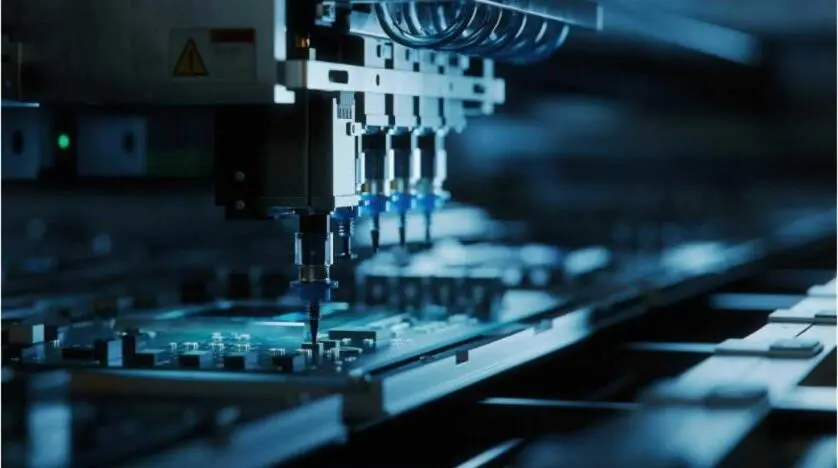
Placement accuracy requirements depend on device type. Optical and RF MEMS typically demand the tightest alignment class. Pressure and fluidic devices may tolerate a wider placement window, but die tilt remains a critical failure mode wherever the sensing element reference plane must remain parallel to the substrate. Pick-and-place head calibration and climate-controlled staging for adhesive cartridges each reduce die tilt. Handling decisions, including pick tool geometry, ejector setup and die presentation format, belong in the placement accuracy specification.
Share placement accuracy and cavity sensitivity requirements with the Pro-Active team.
Domestic MEMS Die Attach For Medical And Defense Sensors
For MEMS programs in regulated industries, domestic sourcing functions as a program risk management decision that reduces IP, counterfeit and supply-chain risks. IP protection, counterfeit avoidance, supply-chain resilience and documentation traceability become harder to enforce across offshore supply chains. ITAR registration is required for any supplier that manufactures, exports or furnishes services related to items on the U.S. Munitions List.
Pro-Active Engineering holds the compliance stack that defense, aerospace and medical MEMS programs require: ISO 9001:2015, AS9100, ITAR registration, JCP certification (DD Form 2345), Nadcap accreditation, NIST 800-171 alignment and CMMC readiness. The facility operates under access controls, data-handling procedures, documentation practices, foreign-national access restrictions per DDTC and personnel training records consistent with ITAR-registered operations. CAGE code 7R4Q2. The facility is located in Sun Prairie, Wisconsin.
AS9100 Rev D adds about 105 requirements beyond ISO 9001:2015, including counterfeit part prevention, configuration management, operational risk management and product safety controls. A supplier holding only ISO 9001 cannot satisfy AS9100 flowdown requirements on flight-critical or safety-critical aerospace programs. Pro-Active holds both certifications.
Prototype-to-production continuity matters for MEMS programs. A process validated in a prototype build should transfer to production without a requalification cycle driven by a supplier change. Pro-Active supports programs from design and rapid prototyping through low- to high-volume production, using the same processes and quality system at every stage.
Engage a domestic, ITAR-registered MEMS die attach partner.
How To Specify A MEMS Die Attach Project
A contract manufacturer needs the following inputs to scope a MEMS die attach project accurately.
-
Die size and material, such as silicon, borosilicate glass or compound semiconductor
-
Substrate or package type, such as ceramic, laminate, metal carrier or direct-to-PCB
-
Attach material preference or constraints, including epoxy class, eutectic, anodic or open to recommendation
-
Required placement accuracy class, such as standard, tight or submicron
-
Cavity or membrane sensitivity, including sealed cavities, exposed membranes, optical paths or fluidic interfaces
-
Downstream interconnect requirements, including wire bonding, flip chip or board-level assembly
-
Volume and ramp expectations, including prototype, low-volume or production
-
Domestic sourcing or compliance requirements, including ITAR, AS9100 or a medical quality system
Evaluation of a MEMS die attach services provider should cover several points. Method-selection experience across epoxy, eutectic and anodic bonding matters. Handling of fragile die pick, ejector setup and cavity protection should be clear. Inspection methods, including optical, acoustic microscopy or X-ray, should match program risk. Documentation and traceability expectations should align with internal requirements. Capability to carry the device through wire bonding, flip chip and board-level assembly without a second vendor reduces handoff risk.
Pro-Active Engineering is an engineering-led, domestic, ITAR-registered partner that integrates MEMS die attach, advanced interconnect, thermal management and PCB assembly in a single workflow. Programs start with a requirements review and move through prototype validation into production without a supplier change.
Use this checklist with purchasing and request a scoped MEMS die attach quote.
Conclusion And Next Steps
The MEMS die attach decision follows a clear framework. Device type determines the viable attach method family. The attach method defines stress and alignment constraints. Those constraints shape the package and board integration path. Skipping steps in that sequence often produces processes that pass initial inspection and fail in the field.
Pro-Active Engineering is a domestic, ITAR-registered partner that carries MEMS die attach through wire bonding, flip chip and board-level integration under one roof, from prototype to production. Founded in 1996, the company operates a facility in Sun Prairie, Wisconsin, with a quality system that includes ISO 9001:2015, AS9100, ITAR registration, JCP certification, Nadcap accreditation, NIST 800-171 alignment and CMMC readiness. As noted earlier, Pro-Active holds the full compliance stack required for regulated MEMS programs.
Recommended next steps include mapping internal requirements with the specification checklist in this guide, shortlisting providers with demonstrated method-selection experience across epoxy, eutectic and anodic bonding and running a pilot or prototype build to validate the attach approach before committing to a production process.
Begin a MEMS die attach project with Pro-Active Engineering.