Key Takeaways for Reliable PCB Panelization
-
Tab-routing with mouse bites delivers the lowest stress depaneling method, avoiding the 5-10% failure rates common with V-scoring in high-reliability prototypes.
-
Use 4-6 tabs per board with 2-3mm mouse bites and 10-15mm courier rails to improve stress distribution and handling.
-
Place at least 3 global fiducials (1-2mm diameter) 5mm from panel edges, plus 2 local fiducials per board, to support precise pick-and-place accuracy.
-
Keep copper distribution variance below 5% across the panel to reduce warping risk, especially on polyimide and heavy copper designs.
-
Pro-Active Engineering’s ITAR-certified Speed Shop delivers DFM-tuned panelization with 2-5 day turnarounds and zero depaneling failures; Request a Quote today.
Why Panelization Matters for High-Reliability Prototypes
High-reliability prototypes in defense, aerospace, and medical programs need panelization strategies that go beyond standard commercial practices. Thin boards under 1.6mm can warp during assembly, and dense layouts increase sensitivity to vibration and depaneling stress. Component failure symptoms during V-scoring depaneling, which causes the 5-10% failure rates noted above, include ceramic capacitor cracking and BGA solder joint micro-cracking when dynamic stress exceeds component tolerance limits.
The reshoring trend and ITAR compliance requirements push teams to work with domestic manufacturing partners who understand these failure modes. Polyimide substrates face thermal-management challenges due to their 0.12 W/m·K thermal conductivity, about one-third of FR-4, which often requires 20-30% de-rating of current-carrying capacity.
For wearable medical devices, maintaining a coefficient of thermal expansion below 20 ppm/°C helps minimize sensor drift. Pro-Active Engineering’s integrated DFM workflow addresses these issues from initial design through production so panelization strategies align with thermal management and assembly needs.
These thermal management considerations become even more critical as flexible printed circuit boards in automotive advanced driver-assistance systems endure temperature excursions from -40°C to +125°C, with the IPC-A-610JA addendum imposing stricter solder-joint acceptance criteria. These demanding specifications call for panelization methods that limit mechanical stress while still supporting automated assembly.
Comparing PCB Panelization Methods for Reliability
Different panelization methods create different stress profiles, so method selection directly affects high-reliability prototype performance. Each option also ties to specific depaneling tools and handling practices.
|
Method |
Reliability Risk |
Depaneling Compatibility |
Prototype Suitability |
|---|---|---|---|
|
Tab-Routing |
Low (no snapping stress) |
Router or manual breakout |
High (flexible, 2-5 days) |
|
V-Scoring |
High (5-10% failure rates) |
Snap, avoid >2.5mm thick |
Low (dense boards) |
|
Laser Scoring |
Very Low |
Laser cutting |
Medium (higher cost) |
Tab routing results in less stress on components during separation compared to V-scoring, especially with well-designed mouse bites. This stress reduction becomes critical in high-density prototypes where components sit closer to panel edges. V-scoring separation can cause stress or microcracks in PCBs if the board thickness exceeds 2.5 mm or if snapping is not controlled.
Pro-Active Engineering’s Speed Shop supports rapid 2-5 day turnaround times for tab-routed prototypes using tightly controlled processes.
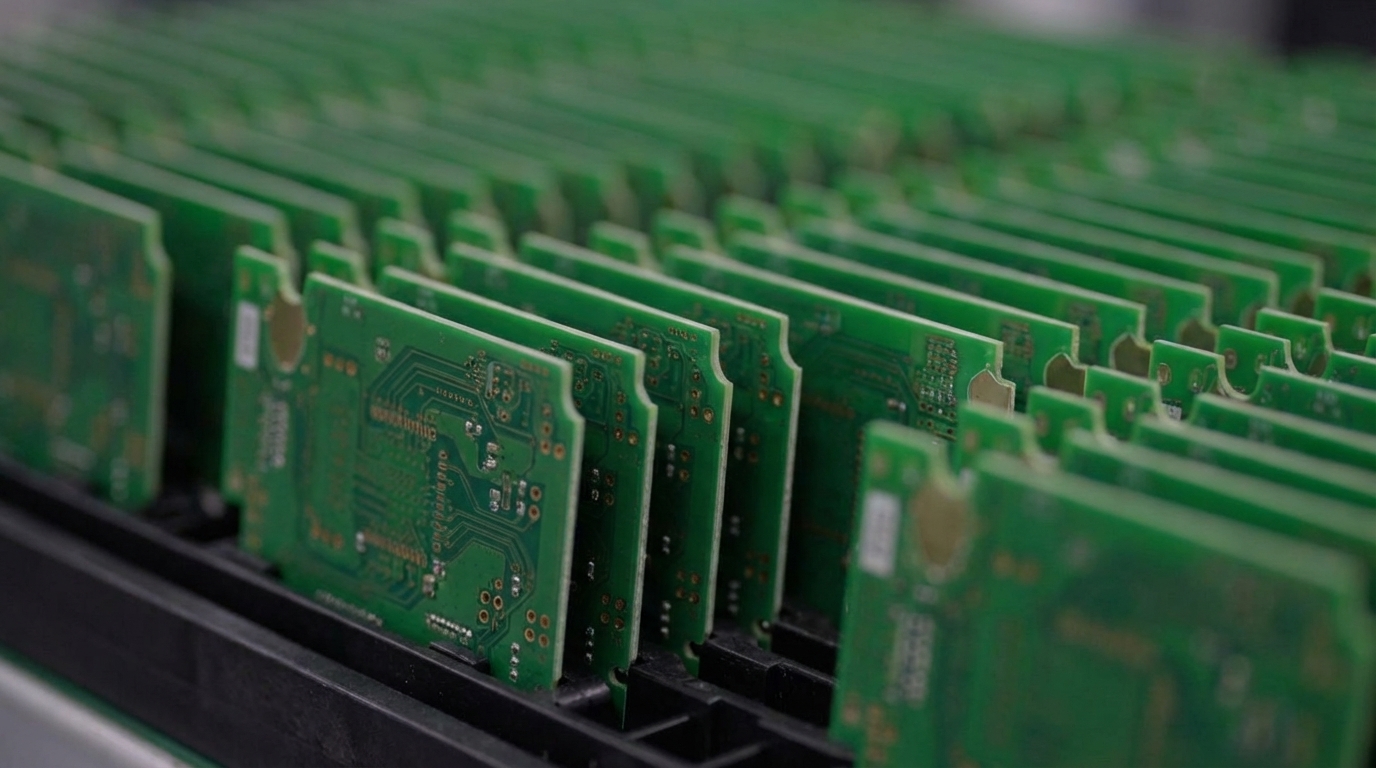
Tab-Routing Strategy with Mouse Bites for Prototypes
Tab-routing with mouse bites offers the most reliable depaneling method for high-reliability prototypes when executed with tight dimensional control. Clear rules for spacing, tab count, and rail design help keep stress away from sensitive components.
Critical Tab-Routing Specifications
-
Mouse bite dimensions: Use the 2-3mm spacing noted earlier with 0.2-0.3 mm holes to facilitate easier tab breaking.
-
Tab quantity: Plan for 4-6 tabs per board to balance rigidity during assembly with low depaneling stress.
-
Courier rail width: Keep 10-15mm rails on all sides to support handling, tooling, and fiducial placement.
-
Tab positioning: Place tabs at board corners and mid-points so stress distributes evenly during breakout.
-
Edge finishing: Use rounded corners to reduce stress concentration and improve handling safety.
Mouse bites in tab routing can sometimes leave small burrs, but Pro-Active Engineering’s controlled router depaneling process removes these consistently. This stress reduction occurs because tab routing eliminates the snapping action that causes the component damage described in the comparison above.
For prototypes that need immediate assembly validation, tab-routing supports same-day depaneling without specialized tooling. This capability aligns with Pro-Active Engineering’s rapid prototyping workflow while still mirroring production-quality processes.
DFM Essentials: Fiducials, Copper Balance, and Keep-Out Zones
High-reliability prototypes depend on precise fiducial placement and copper balancing to maintain automated assembly accuracy and thermal stability. These rules carry forward directly when the design scales to production.
Fiducial Requirements for Automated Pick-and-Place
-
Quantity: Use a minimum of 3 global fiducials per panel plus 2 local fiducials per board.
-
Size: Keep fiducials between 1mm and 2mm in diameter for standard vision systems.
-
Placement: Position fiducials at least 5mm from panel edges and outside component keep-out zones.
-
Material: Use bare copper with HASL or ENIG finish to create strong optical contrast.
Copper Balancing Specifications: Maintain copper distribution variance below 5% across the panel to limit warping during reflow. This requirement becomes especially important for polyimide substrates with coefficient of thermal expansion below 20 ppm/°C for wearable medical devices.
Component-Free Zones: V-scoring requires a minimum keep-out distance of 0.5mm to 1mm for components, traces, or pads from the score line. Tab-routing allows components closer to board edges, but maintain at least 5mm clearance from tab locations.
Request a Quote for DFM-Optimized High-Reliability Prototypes
Advanced Panelization for Thermal and High-Density Designs
High-density prototypes in defense and aerospace programs need advanced thermal management during panelization. Copper balancing shapes thermal distribution, while component density influences which depaneling method makes sense.
Pro-Active Engineering’s silver sintering and direct thermal path PCB technologies rely on specialized panelization approaches. Heavy copper layers and thermal vias create asymmetric stress patterns, so engineers use strategic tab placement and copper balancing to counter those forces. Component layout guidelines specify keep-out areas of ≥3.0mm for BGA packages to avoid solder joint fatigue.
Advanced fiducial strategies now use AI-optimized placement algorithms that factor in component density and the polyimide thermal expansion characteristics mentioned earlier. Boyd Corporation recommends polyimide films with a coefficient of thermal expansion below 20 ppm/°C for wearable medical devices to minimize sensor drift, which drives corresponding adjustments to panelization stress analysis.
For high-frequency applications, high-frequency signal lines must be maintained at least 3mm from V-groove edges to prevent impedance discontinuity. Tab-routing improves RF prototype performance by removing groove-induced impedance variations.
DFM Checklist for High-Reliability PCB Panelization
This checklist guides first-pass panelization success for high-reliability prototypes and follows the same order as a typical layout review.
-
Tab Design Verification: Confirm 2-3mm mouse bites with 4-6 tabs per board to control depaneling stress while keeping panels rigid enough for assembly.
-
Fiducial Placement: After tab locations are set, verify 3 global fiducials positioned at least 5mm from panel edges so they do not interfere with depaneling areas.
-
Copper Balance Analysis: With the physical layout defined, ensure copper distribution variance remains below 5% to reduce thermal warping during reflow.
-
Component Clearances: Check that components maintain at least 5mm clearance from depaneling areas to protect BGAs and ceramics from breakout stress.
-
Thermal Considerations: Review CTE mismatch in multi-material stackups so panelization does not amplify bow and twist.
-
Depaneling Method Selection: Match method to thickness and density, and avoid V-scoring for boards thicker than 2.5mm.
-
Post-Depanel Inspection: Plan AOI and functional testing protocols that specifically target solder joints and components near separation lines.
EMS-led Design for Manufacturability improves panelization and routing efficiency, reduces prototype spins, and avoids late-stage Engineering Change Orders. Pro-Active Engineering’s integrated DFM review process addresses these checklist items during initial design consultation to prevent costly redesigns.
Defense Prototype Case Study: Zero-Failure Depaneling
A recent ITAR-classified defense prototype program showed how optimized panelization improves first-pass yield. The project used high-density RF boards with BGA components that required zero-failure depaneling for mission-critical use.
Pro-Active Engineering’s approach combined tab-routing with precision mouse bites, strategic copper balancing for thermal control, and automated router depaneling. The Speed Shop delivered functional prototypes in 3 days with 100% depaneling success, which allowed immediate system integration testing. AS9100 quality processes then supported a smooth transition to production volumes with consistent yield.
The integrated engineering workflow removed two potential redesign cycles by addressing panelization constraints during the initial layout review. Design for Excellence delivers predictable yields and defined test times early in the New Product Introduction process, enabling better cost models and reducing post-launch surprises.
Request a Quote for DFM-Optimized High-Reliability Prototypes
Conclusion: A Practical Panelization Playbook
The most effective PCB panelization strategy for high-reliability prototypes uses tab-routing with mouse bites, strategic fiducial placement, and tight copper balancing. This combination reduces the 5-10% failure rates linked to improper depaneling and still supports fast prototype turnaround. Pro-Active Engineering’s ITAR-certified Speed Shop applies these DFM principles along with advanced thermal management and automated depaneling to deliver smooth prototype-to-production transitions for mission-critical applications.
Frequently Asked Questions
What are the key differences between tab-routing and V-scoring for high-reliability prototypes?
Tab-routing with mouse bites creates significantly less mechanical stress during depaneling compared to V-scoring, which can cause microcracks and component damage. V-scoring relies on snapping action that generates dynamic stress, while tab-routing allows controlled separation through router cutting or careful manual breakout.
For high-reliability applications, tab-routing offers better protection for sensitive components like BGAs and ceramic capacitors. Tab-routing also handles boards thicker than 2.5mm more effectively, while V-scoring becomes problematic above this thickness.
How do fiducial requirements differ for prototype versus production panelization?
Prototype panelization uses the same fiducial precision as production so assembly validation reflects real manufacturing conditions.
A minimum of 3 global fiducials per panel plus 2 local fiducials per board supports accurate pick-and-place alignment. Fiducials should be 1-2mm in diameter, positioned at least 5mm from panel edges, and finished with bare copper for strong optical contrast. The main difference in prototyping is confirming that fiducial placement supports current assembly and future production scaling without layout changes.
What copper balancing specifications are critical for thermal management in high-power prototypes?
Copper distribution variance should remain below 5% across the panel to prevent thermally driven warping during assembly. This requirement becomes especially important for high-power designs that use heavy copper layers or dedicated thermal features. Copper balancing affects mechanical stability during reflow and long-term thermal performance. For polyimide-based flexible circuits, lower thermal conductivity compared to FR-4 demands even more careful copper distribution planning to control thermal gradients.
How does panelization strategy affect prototype-to-production transition timelines?
Robust panelization strategy during prototyping removes the need for redesign when scaling to production volumes. Tab-routing with standardized mouse bite dimensions and consistent fiducial placement transfers directly to production tooling without modification.
Poor initial panelization choices can add 2-4 weeks to production transition timelines due to layout changes and new tooling. Pro-Active Engineering’s integrated approach keeps prototype panelization aligned with long-term volume goals so teams can scale from single units to thousands without extra design spins.
What are the most common panelization failures in defense and aerospace prototypes?
Common failures include component cracking from excessive depaneling stress, solder joint damage from improper V-scoring, warping from unbalanced copper distribution, and assembly misalignment from weak fiducial strategies. BGA packages face higher risk of solder joint fatigue when placed too close to separation lines.
Ceramic components can crack under dynamic stress during manual snapping. These issues are avoidable through well-executed tab-routing, clear keep-out zones, and controlled depaneling processes that remove manual snapping stress.