Key Flip Chip Advantages for Complex Electronics
-
Flip chip packaging mounts the die face-down using solder bumps or copper pillars, which shortens electrical paths and improves signal integrity at high frequencies.
-
The architecture creates a direct thermal path from the die backside to heat spreaders, supporting efficient heat dissipation in high-power aerospace, defense and medical applications.
-
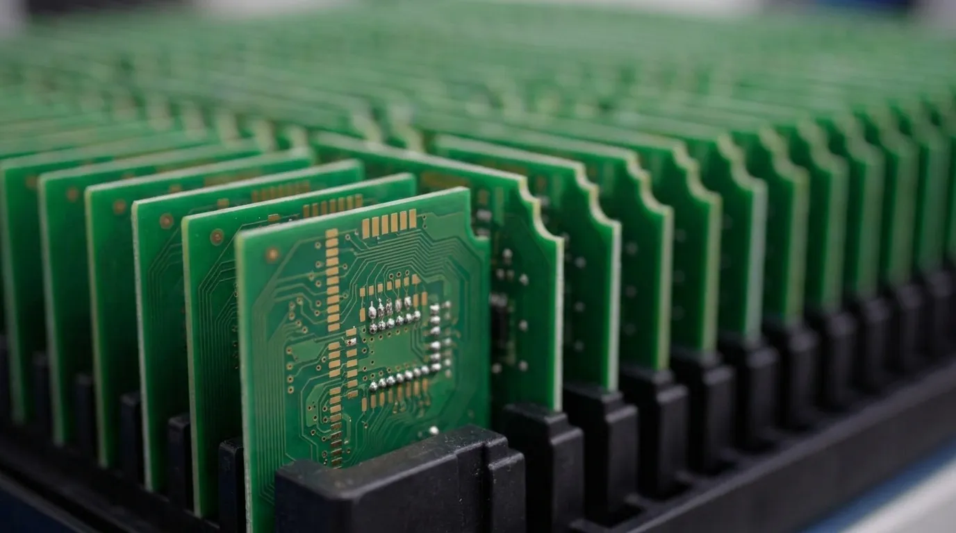
Area-array I/O distribution across the full die surface increases interconnect density and reduces package footprint compared to perimeter wire bonding.
-
Eliminating wire loops improves long-term reliability under vibration, shock and thermal cycling, supporting qualification standards for regulated environments.
-
Pro-Active Engineering integrates DFM, advanced interconnect assembly and full documentation control under one domestic workflow; connect with the team to discuss flip chip packaging requirements.
Core Benefits of Flip Chip Packaging
High-Frequency Electrical Performance
Wire bonds introduce parasitic inductance and impedance that degrade signal integrity as operating frequencies rise. Flip chip interconnects are shorter and more direct, which reduces these parasitics at the package level.
Flip chip MicroLeadFrame packages using copper pillar bumping demonstrate low simulated inductances for representative die and body sizes. The same source reports that flip chip MLF devices show simulated package impedances lower than wire-bond MLF devices at 500 MHz and 1 GHz. Amkor’s flip chip MicroLeadFrame platform operates at 20 GHz or higher and maintains strong signal integrity through flip chip interconnects.
These performance characteristics matter in demanding RF systems. For radar, electronic warfare, software-defined radio and high-speed data acquisition systems, this impedance advantage translates into cleaner signal paths, reduced crosstalk and more predictable behavior at millimeter-wave frequencies. Achieving these benefits in production requires early DFM planning that addresses bump pitch, substrate routing and ground return paths before layout is finalized.
Thermal Management for High-Power Designs
Flip chip architecture improves thermal paths for high-power devices. In wire-bonded packages, heat generated at the die must travel through the die attach material and substrate before reaching a heat spreader or heatsink.
Flip chip configurations orient the back of the die upward, which enables direct attachment of a lid or heat spreader with a thermal interface material in a shorter, lower-resistance path. Advanced TIM materials used in flip chip lidded ball grid array packages demonstrate the thermal performance this architecture enables. Indium-silver alloys used as TIMs in flip chip packages exhibit thermal conductivities ranging from 71 to 86 W/m·K depending on silver content, which supports efficient heat transfer from the die to the heat spreader in large-body, high-power packages.
The same research, conducted with Amkor Technology, found that all five indium-silver alloy variants with thermal conductivity above 71 W/m·K delivered stable junction-to-case thermal resistance at end-of-line testing and showed slightly improved results after long-term reliability testing, including high-temperature storage and temperature cycling.
This combination of high thermal conductivity and proven reliability under stress makes flip chip architecture suitable for demanding applications. For high-power RF amplifiers, power management ICs and processing units in aerospace and defense platforms, this thermal approach supports sustained operation where wire-bonded packages might require larger footprints or added cooling hardware to reach similar junction temperatures.
I/O Density and Package Footprint
Flip chip packaging increases I/O density while shrinking package size. Wire bonding places interconnects around the perimeter of the die, which limits I/O count as die sizes shrink.
Flip chip distributes bumps across the entire active surface of the die and enables area-array I/O configurations that scale with die complexity rather than perimeter length. Amkor’s flip chip MicroLeadFrame packages achieve smaller package sizes than traditional wire-bonded MicroLeadFrame packages of the same die size. That footprint reduction is significant for board-level density in avionics, satellite payloads and implantable or wearable medical devices where board area and mass are constrained.
Beyond enabling smaller packages, higher I/O density also supports heterogeneous integration strategies. RF GaN packaging for defense, aerospace and satellite communication applications increasingly incorporates flip chip alongside fan-out wafer-level packaging and system-in-package solutions, as identified in the Global RF GaN Market 2026-2036 report. The early DFM attention mentioned earlier becomes especially critical for heterogeneous integration, where substrate design rules, material choices and inspection plans must align across multiple technologies.
Long-Term Reliability in Regulated Environments
Flip chip packages improve mechanical robustness for harsh environments. Wire loops are susceptible to vibration-induced fatigue, bond-lift failure and corrosion at the bond interface.
Flip chip replaces these loops with an area-array of solder bump or copper pillar interconnects that distribute mechanical stress more uniformly across the package. That stress distribution matters for platforms subject to shock, vibration and thermal cycling.
Reliability qualification for flip chip packages in mission-critical applications follows established stress protocols. Flip chip package TIM performance has been validated through high-temperature storage and temperature cycles under K condition, with junction-to-case thermal resistance measured on internal thermal test vehicles. Reliability testing of packaged semiconductor devices evaluates performance against high temperature, humidity, temperature cycling, mechanical vibration and high-voltage stresses, including accelerated life tests that screen for early failures and validate long-term lifespan.
For aerospace, defense and medical programs operating under AS9100, MIL-SPEC or FDA quality frameworks, this qualification data supports design decisions and documentation packages. Those decisions must account for factors that directly affect long-term solder joint reliability; underfill selection, bump metallurgy and substrate CTE matching all require engineering input during the design phase.
Connect with Pro-Active Engineering’s team to discuss flip chip reliability requirements for regulated programs.
Manufacturing Feasibility for Flip Chip Programs
Successful flip chip implementation depends on manufacturing readiness. Flip chip assembly introduces process variables such as bump inspection, flux management, underfill dispensing and cure, and post-assembly X-ray verification. These steps require manufacturing infrastructure and process discipline beyond standard SMT assembly.
Programs that treat packaging selection as a late-stage decision often encounter redesign cycles when substrate design rules, underfill compatibility or inspection access are not addressed during layout. Early collaboration between design and manufacturing reduces this risk and keeps schedules on track.
Pro-Active Engineering integrates DFM into the design phase for flip chip programs. Engineering and manufacturing operate within a single workflow, which means substrate routing rules, bump pitch constraints and underfill process windows are evaluated before layout is finalized. Full documentation control and traceability are maintained throughout, which supports the audit and reporting requirements of aerospace, defense and medical programs.
Pro-Active Engineering holds the certifications required for defense and aerospace programs, including AS9100, ITAR registration and Nadcap accreditation, with all advanced interconnect work performed domestically.
When Flip Chip Packaging Fits Program Requirements
Flip chip packaging suits programs with specific performance and reliability needs. Typical drivers include operating frequencies above several hundred MHz where parasitic inductance and impedance degrade signal integrity, and high power density where junction temperature management is a design constraint.
Additional drivers include I/O counts that exceed what perimeter wire bonding can support at the required die size, board-level footprint or mass constraints, and long service life in environments involving vibration, thermal cycling or humidity exposure. Programs without these conditions often select wire bonding as a simpler and more cost-effective option at lower complexity levels.
Partner With Pro-Active Engineering for Flip Chip Solutions
Pro-Active Engineering delivers flip chip packaging as part of an integrated U.S. design-to-production workflow. From DFM through assembly, test and full documentation, programs benefit from a single accountable domestic partner with the certifications and process infrastructure that aerospace, defense and medical applications require.
This integrated approach, combined with full certification coverage and domestic operations, positions Pro-Active Engineering as a single accountable partner for flip chip programs. Start the conversation with Pro-Active Engineering’s advanced interconnect team about flip chip requirements.
Frequently Asked Questions
What is the difference between flip chip and wire bonding?
Wire bonding connects a face-up die to its package using thin metal wires looped from bond pads on the die perimeter to corresponding pads on the substrate or leadframe. Flip chip inverts the die and connects it face-down to the substrate through solder bumps or copper pillars distributed across the active surface.
The primary differences involve interconnect length, I/O placement, thermal path geometry and susceptibility to vibration-induced fatigue. Flip chip provides shorter electrical paths, area-array I/O capability and a direct thermal path from the die backside to a heat spreader, while wire bonding is simpler to implement and remains cost-effective for lower-complexity, lower-frequency designs.
How does flip chip compare to BGA packaging?
Ball grid array packaging uses solder balls on the underside of a packaged component to connect to the PCB. Flip chip is an interconnect method at the die level, where the bare die connects directly to a substrate without a traditional package body.
Flip chip can be implemented within a BGA-style package, such as a flip chip BGA, which combines area-array board-level connectivity with the electrical and thermal advantages of direct die attachment. The distinction matters for engineers who evaluate where in the assembly hierarchy the interconnect performance gains are needed, at the die-to-substrate level, the component-to-board level or both.
What manufacturing certifications are relevant for flip chip programs in aerospace and defense?
Aerospace and defense flip chip programs typically require suppliers to hold AS9100 certification for quality management, ITAR registration for controlled technology handling and documentation, and Nadcap accreditation for special processes. JCP certification covers military and government electronics requirements. IPC-A-610 Class 3 workmanship standards apply to high-reliability assemblies.
Programs with controlled unclassified information may also require NIST 800-171 alignment or CMMC readiness. Pro-Active Engineering holds all of these credentials and applies them across its advanced interconnect and packaging work.
When does flip chip packaging make sense over wire bonding from a DFM perspective?
Flip chip becomes the preferred interconnect strategy when the design requires high I/O density that perimeter wire bonding cannot support at the target die size, when operating frequencies demand lower parasitic inductance and impedance than wire bonds provide, or when thermal resistance must be minimized for high-power operation.
DFM considerations include substrate design rules compatible with bump pitch, underfill material selection for the target thermal and mechanical environment, and inspection access for post-assembly X-ray verification. Engaging manufacturing engineering during the design phase, rather than after layout is complete, reduces the risk of late-stage redesign and process incompatibilities.
Can flip chip assembly be performed domestically with full ITAR compliance?
Domestic flip chip assembly with ITAR compliance is available through suppliers that hold ITAR registration and maintain controlled facility and documentation practices. For defense and aerospace programs, domestic manufacturing removes the export control exposure associated with sending controlled designs or hardware to offshore assembly operations.
Pro-Active Engineering performs flip chip assembly at its Wisconsin facility under ITAR-registered, AS9100-certified and Nadcap-accredited conditions, with full traceability and documentation control maintained throughout the program lifecycle.