Last updated: April 17, 2026
Key Takeaways
- High-Tg FR-4 materials (≥170°C) with CTE-matched properties reduce via fractures and delamination during thermal cycling.
- Symmetrical stackups with balanced copper distribution limit bow and twist to 0.75% per IPC-6012 for reliable surface mount assembly.
- IPC Class 3 requires ≥0.05mm annular rings with fabrication allowances that protect via integrity under mechanical stress.
- Filled thermal vias and silver sintering create direct heat paths that improve reliability in high-power mission-critical designs.
- Pro-Active Engineering delivers DFM-focused high-rel PCB assemblies with 2-5 day prototyping and 100% AOI; get a tailored quote for seamless prototype-to-production.
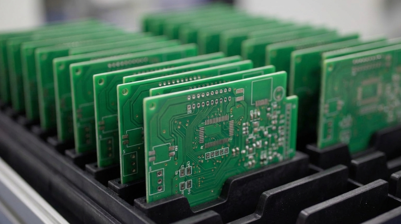
1. Material Selection for High-Reliability PCB Manufacturing
High-reliability PCB assemblies start with materials engineered for thermal stability and dimensional control. High-Tg FR-4 materials with glass transition temperatures of 170°C or higher provide closer CTE matching in X/Y directions compared to standard FR-4. This closer match to copper reduces thermal cycling stress and lowers the risk of via fractures during reflow soldering. FR-4 TG170 or FR4-H grade materials also limit thermal expansion-induced pad cracking and interlayer delamination in mission-critical designs. Pro-Active Engineering specifies high-Tg laminates for all Class 3 assemblies to maintain reliability under extreme operating conditions and to support the stackup strategies that follow.
2. Symmetrical PCB Stackup for Dimensional Stability
Balanced layer construction controls warpage and dimensional instability in high-reliability assemblies. To achieve this balance, symmetric stackups distribute copper evenly across layers and limit bow and twist to 0.75% per IPC-6012 for surface mount boards. Copper balancing techniques using patterned copper dots or segmented regions create mechanical symmetry and prevent warpage during lamination. Pro-Active Engineering’s symmetrical builds combine balanced copper weights with controlled resin content so boards remain flat through thermal cycling and assembly. This stable foundation supports reliable vias, pads, and thermal structures in the next design steps.
3. IPC Class 3 Annular Rings and Pad Design Details
Annular ring integrity forms the foundation of reliable interconnections in Class 3 assemblies. IPC-2221 specifies minimum annular ring dimensions of 0.05mm for Class 3 high-reliability electronic products, with added fabrication allowance for drill misalignment and etching tolerances. Class 3 standards allow maximum misalignment of ±2 mil, with all layers inspected using X-rays to verify concentricity. Pro-Active Engineering builds in generous fabrication allowances and uses rounded trace connections so pad-to-trace transitions handle both thermal and mechanical stress. These robust connections then support the thermal and mechanical roles that vias play in the next stage of the design.
4. Thermal Management Vias in High-Rel Assemblies
Thermal via design creates predictable heat paths that protect components and solder joints. IPC-6012 provides guidelines for void volume in filled vias, including via-in-pads and stacked microvias, to maintain consistent thermal conduction. Silver sintering in die-attach operations delivers high heat conductivity and strong mechanical bonds for demanding thermal cycling applications. Pro-Active Engineering’s thermal via structures use filled vias with direct copper paths and advanced sintering techniques to move heat efficiently away from power devices. These thermal strategies work alongside placement decisions that further control hotspots and mechanical stress.
5. Component Placement Guidelines for Reliable Assembly
Strategic component placement reduces thermal hotspots and simplifies manufacturing. High-density designs use 10-20 mil spacing between components to maintain clearance for assembly processes and thermal expansion. Power components receive extra attention and are positioned away from board edges, then distributed across the board to avoid localized heating. Large, heavy, or power components placed away from edges and corners experience lower bending stresses, which reduces solder joint fatigue. Pro-Active Engineering’s placement guidelines combine thermal modeling and stress analysis so component locations support both reliability and manufacturability before routing begins.
6. Trace Routing Rules for Class 3 PCB Designs
Trace geometry directly affects signal integrity and manufacturing yield in high-reliability designs. IPC Class 3 PCBs with 1 oz copper require trace widths and spacing that match current capacity and voltage clearance needs. Class 3 design rules recommend teardrops at pad-to-trace junctions to prevent cracks around vias and pads. High-speed signal paths rely on controlled impedance and matched differential pairs to preserve signal quality. Pro-Active Engineering’s routing standards apply advanced design rules for high-speed, high-density interconnects with carefully tuned trace geometries. Once routing is stable, the design can support accurate assembly through well-planned fiducials and panelization.
7. Fiducials and Panelization for Assembly Accuracy
Accurate fiducial placement enables repeatable automated assembly and inspection. Global fiducials require board or panel edge clearance greater than 4.75 mm (187 mils) plus the fiducial mark clearance so pick-and-place systems can see them reliably. Local fiducials near fine-pitch components add registration accuracy for critical placements. Panel design includes tooling holes and breakaway tabs while preserving enough rigidity for handling during assembly. Pro-Active Engineering’s 100% AOI inspection depends on these optimized fiducial and panelization strategies to maintain consistent placement accuracy across every build. With mechanical and optical alignment in place, the focus shifts to solder mask and markings that support clean assembly.
8. Solder Mask and Silkscreen Tolerances for Class 3
Careful solder mask and silkscreen control prevents assembly defects and supports long-term reliability. Solder mask openings need enough clearance around pads to allow proper solder flow while avoiding exposure of adjacent traces that could cause bridging. Silkscreen legends require minimum clearances from pads and vias so ink does not contaminate solderable surfaces during assembly. IPC Class 3 standards work together with J-STD-001 to define these soldering and cleanliness requirements. Pro-Active Engineering’s mask and silkscreen specifications use tight tolerances and high-resolution printing so component identification stays clear and assembly remains consistent. These visual and protective layers then support efficient testing and inspection.
9. Test Points and Inspection Integration for Class 3
Comprehensive test access allows thorough verification and quality control. Test points need sufficient spacing and accessibility for flying probe and in-circuit testing equipment. Via-in-pad structures must preserve testability while still delivering strong thermal performance. Boundary scan and JTAG access points simplify board-level testing and debugging on dense designs. Pro-Active Engineering combines full traceability with inspection protocols that include flying probe testing and functional verification so every assembly meets Class 3 reliability standards before shipment. With robust test coverage in place, advanced features can safely increase density and performance.
10. Advanced Features for Mission-Critical High Density
High-density interconnect technologies support compact, high-performance assemblies without sacrificing reliability. IPC-2226 HDI standard specifies minimum microvia annular rings of 0.025mm for Level A designs and 0.015mm for Level C high-density designs. Wire bonding and flip chip assembly create short, direct electrical connections that reduce parasitic effects. Si3N4 ceramic substrates reach thermal conductivities up to 169 W·m⁻¹·K⁻¹ while maintaining high fracture toughness for power electronics. Pro-Active Engineering’s advanced interconnect capabilities include wire bonding, flip chip assembly, and hybrid packaging that support mission-critical applications requiring maximum performance density.
Why Pro-Active Engineering Excels in High-Reliability PCB DFM
Pro-Active Engineering operates as a single-source partner for DFM-focused high-reliability assemblies through tightly integrated engineering and manufacturing workflows. Our end-to-end capabilities cover PCB design and layout, rapid 2-5 day prototyping through the Speed Shop, advanced assembly with 100% AOI inspection, and complete box build integration. With ISO 9001:2015, AS9100, ITAR, and Nadcap certifications, we maintain controlled processes and full traceability for mission-critical programs. Our single-location model removes handoff risks common with fragmented offshore supply chains and supports smooth transitions from prototype to production. More than 30 years of experience in defense, aerospace, and medical electronics, combined with advanced thermal management and silver sintering technologies, help reduce redesign cycles and shorten time-to-market for complex assemblies.
Downloadable PCB DFM Checklist for Design Reviews
Effective DFM verification relies on a structured review of design parameters and manufacturing requirements. Our downloadable checklist consolidates the key specifications covered throughout this article, including material choices, stackup symmetry, thermal via validation, and Class 3 feature requirements, into a single review tool. Additional items address component placement clearances, trace width and spacing, fiducial positioning, test point accessibility, and solder mask tolerances. Pro-Active Engineering uses this checklist during collaborative design reviews to surface potential issues early in development. This approach supports first-pass manufacturing success and consistent high-reliability performance.
Frequently Asked Questions
What defines IPC Class 3 DFM requirements for high-reliability PCBs?
IPC Class 3 DFM requirements set the highest reliability standards for mission-critical electronics. These requirements include minimum annular rings of 0.05mm, copper plating thickness of 25μm in via barrels, zero tolerance for annular ring breaks, and strict dimensional controls. Class 3 designs must endure extended thermal cycling, mechanical stress, and harsh environmental conditions. Materials need glass transition temperatures above 170°C, and assembly processes must comply with J-STD-001 Class 3 standards. Pro-Active Engineering maintains compliance through integrated design reviews and tightly controlled manufacturing processes.
How do you prevent CTE mismatch issues in high-reliability assemblies?
CTE mismatch control begins with careful material selection and stackup planning. High-Tg FR-4 materials align more closely with copper’s 17 ppm/°C expansion rate than standard FR-4, which reduces stress at interfaces. Symmetrical stackups with balanced copper distribution further limit warpage during thermal cycling. Component selection favors parts with CTE values closer to the PCB substrate, and layout places large components away from board edges where thermal stress concentrates. Pro-Active Engineering specifies appropriate materials and validates thermal performance through detailed testing protocols.
What are the best practices for prototype DFM validation?
Prototype DFM validation works best when manufacturers join the design process early. Rapid prototyping that uses production-equivalent processes exposes manufacturability issues before volume builds. Key validation steps include design rule checks against Class 3 standards, thermal modeling for power dissipation, signal integrity analysis for high-speed paths, and assembly simulation to refine component placement. Pro-Active Engineering’s Speed Shop delivers production-ready prototypes in 2-5 days using the same processes and materials as full production. This alignment supports seamless scaling and prevents prototype-to-production disconnects.
How do thermal vias improve reliability in high-power assemblies?
Thermal vias create direct conduction paths that move heat from power components to heat sinks or ground planes. Filled vias provide consistent thermal performance and remove air gaps that would otherwise reduce heat transfer. Silver sintering and advanced fill materials further increase thermal conductivity beyond standard copper plating alone. Effective thermal via design includes sufficient via density under power devices, solid connections to thermal planes, and via diameters and spacing tuned to the power profile. Pro-Active Engineering’s thermal management expertise covers advanced via filling and direct thermal path PCB technology to maximize heat dissipation efficiency.
What inspection methods ensure Class 3 quality standards?
Class 3 quality assurance depends on layered inspection throughout manufacturing. Automated Optical Inspection (AOI) checks component placement, solder joint quality, and surface defects. X-ray inspection examines internal solder joints and via fill quality. In-circuit testing verifies electrical connectivity and component values, while flying probe testing offers flexible coverage for complex or low-volume designs. Microsection analysis confirms copper plating thickness and via barrel integrity. Pro-Active Engineering applies 100% AOI and uses statistical sampling for advanced inspection methods so every assembly meets Class 3 reliability expectations.
Applying these 10 DFM principles for high-reliability PCB assemblies supports mission-critical performance and consistent manufacturing outcomes. Pro-Active Engineering’s integrated approach combines advanced design capabilities, rapid prototyping, and controlled manufacturing to deliver assemblies that exceed Class 3 requirements. Connect with our engineering team to discuss your high-reliability requirements and receive a detailed quote.