Key Takeaways for Advanced Flip Chip Packaging
- Advanced flip chip packaging bonds dies face-down to substrates with solder bumps or copper pillars, which increases I/O density and electrical performance over wire bonding.
- The process follows six steps: wafer bumping, dicing, alignment, reflow, underfill and testing, with design for manufacturability planning that improves yield and reliability.
- Flip chip outperforms wire bond and BGA in signal integrity, thermal management and reduced package size suited to defense and aerospace systems.
- Challenges such as underfill voids and thermal mismatch are managed through advanced materials, tight process control and integrated engineering support.
- Pro-Active Engineering provides end-to-end flip chip design, prototyping and assembly with certifications for regulated industries; connect with our engineering team for seamless support.
Advanced Flip Chip Packaging Explained
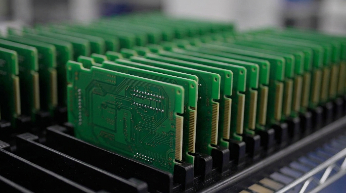
Advanced flip chip packaging bonds a semiconductor die face-down directly to a substrate with solder bumps or copper pillars, which improves I/O density and electrical performance compared to traditional wire bonding methods. This direct attachment approach removes bond wires and creates area-array interconnects that support higher pin counts in a smaller footprint.
Core characteristics of advanced flip chip packaging include high-density area-array interconnects that maximize I/O utilization, shorter signal paths that reduce inductance and improve signal integrity, superior heat transfer through direct thermal conduction and finer pitches below 40 micrometers for next-generation applications. These capabilities have driven the evolution from traditional controlled collapse chip connection (C4) processes to advanced copper pillar and hybrid bonding approaches, which support compact, high-performance electronics in regulated industries.
The Flip Chip Packaging Process in Six Steps
The advanced flip chip packaging process follows six critical steps that build reliable interconnections and consistent performance.
1. Wafer bumping: Copper pillar formation is widely used in the bump type segment</a. This step creates the interconnect structures on the semiconductor wafer.
2. Dicing and flux application: Individual dies separate from the wafer. Flux materials support proper reflow and strong joint formation.
3. Die flip and alignment: The semiconductor die inverts and aligns precisely with the substrate. Advanced vision systems and placement equipment maintain accurate alignment.
4. Reflow process: Thermocompression bonding (TCB) provides reliable interconnections for fine-pitch applications. Mass reflow and TCB processes support advanced performance requirements.
5. Underfill encapsulation: Advanced underfill materials offer higher thermal conductivity. This step reduces mechanical stress and strengthens long-term reliability.
6. Lid attach and testing: Final assembly steps include thermal interface material application, lid attachment and comprehensive electrical testing. These tests confirm that devices meet performance specifications.
Throughout these process steps, design for manufacturability considerations remain critical to success. Design for manufacturability planning covers substrate selection for thermal expansion matching, bump pitch choices that improve yield and thermal management strategies. Pro-Active Engineering applies an integrated engineering approach to these DFM requirements from the initial design phase. This approach reduces costly redesigns and shortens time to market.
Flip Chip, Wire Bond and BGA Compared
Advanced flip chip packaging delivers clear advantages over traditional wire bonding and ball grid array (BGA) approaches. Flip chip packages deliver smaller form factors compared to wire-bonded alternatives while also improving signal integrity. These combined benefits make flip chip well suited to space-constrained defense and aerospace applications.
Electrical performance improvements include lower inductance values that support high-speed designs. Flip chip MicroLeadFrame packages can achieve lower parasitic inductance than wirebond MLF packages. These packages enable superior signal integrity in high-frequency applications. The reduction in inductance also improves electromagnetic interference suppression and power delivery.
Thermal management provides another key advantage and builds on the electrical benefits. Advanced flip chip packages achieve lower junction-to-board thermal resistance than wirebond MLF packages. These packages provide stronger heat dissipation for high-power applications.
The distinction between flip chip and BGA packaging centers on the direct die attachment approach. BGA packages use an intermediate substrate layer between the die and the printed circuit board. Flip chip technology bonds the die directly to the final substrate. This structure removes one level of interconnection and reduces overall package height and thermal resistance.
Benefits and Use Cases in High-Performance Industries
Advanced flip chip packaging supports mission-critical applications across defense, aerospace and medical device industries. The reduced package size enables higher component density on printed circuit boards. This density supports miniaturization trends in portable and embedded systems.
Enhanced reliability results from the removal of bond wires. Bond wires create potential failure points under vibration and thermal cycling conditions. This reliability advantage becomes especially important in aerospace electronics, which endure vibration and temperature extremes. Copper pillar bumps and ultra-thin substrates maintain mechanical robustness for high-density packaging even under these demanding conditions.
Scalability advantages support both prototype and production requirements. North America supports domestic assembly of flip chip units, driven by demand from data centers, defense and medical devices that require ITAR-compliant or regulated manufacturing.
Key applications include defense electronics that require ITAR-compliant manufacturing and vibration resistance. Aerospace systems demand long-term reliability under extreme conditions. Medical devices benefit from smaller footprints and biocompatible materials. Power electronics gain from strong thermal management capabilities. Pro-Active Engineering’s experience in these regulated industries supports compliance with strict quality and documentation requirements.
Challenges in Advanced Flip Chip Packaging and Practical Solutions
Manufacturing challenges in advanced flip chip packaging call for specialized expertise and proven solutions. Underfill void formation represents a primary concern because trapped air or incomplete flow creates reliability issues under thermal cycling. Advanced process control and optimized underfill materials address this challenge by improving flow characteristics and reducing cure times.
Thermal mismatch between different materials in the package stack generates mechanical stress and potential failure modes. Solution approaches include careful material selection, thermal interface improvements and design changes. These changes accommodate thermal expansion differences and reduce stress on solder joints.
Yield improvement depends on integrated testing and process monitoring throughout the assembly sequence. Integration of machine learning and AI in flip chip assembly optimizes processes for high-volume production environments.
Pro-Active Engineering addresses these challenges through design-for-manufacturability integration from day one, comprehensive thermal management solutions and advanced process control systems. The company’s 30-plus years of experience in high-reliability electronics manufacturing supports successful flip chip implementation across demanding applications.
Why Pro-Active Engineering Leads in Flip Chip Packaging
Pro-Active Engineering operates as a leading Wisconsin-based PCBA manufacturer with comprehensive flip chip, wire bond and hybrid assembly capabilities. The company’s integrated workflow removes the vendor fragmentation that creates communication gaps and increases program risk in complex electronics development.
Rapid prototyping through the dedicated Speed Shop supports fast iteration cycles that advanced packaging development requires. Production-ready prototypes built with full manufacturing processes create a smooth transition to volume production without costly redesigns or process changes.
Comprehensive certifications including ISO 9001:2015, AS9100, ITAR registration, JCP certification and Nadcap accreditation demonstrate the quality management systems required for mission-critical applications. These certifications provide the documentation control and traceability essential for defense and aerospace programs.
End-to-end capabilities reduce supply chain complexity compared to offshore or fragmented provider models. From initial PCB design and firmware development through advanced packaging, testing and system integration, Pro-Active Engineering delivers accountable partnership throughout the product lifecycle. Start a flip chip consultation with our packaging specialists for integrated manufacturing support.
Future Trends in Advanced Flip Chip Technology
The global flip chip market grows as demand increases for high-performance computing and AI applications.
Finer-pitch copper pillar technology advances toward sub-10 micrometer interconnects. Hybrid bonding technologies combine thermocompression and mass reflow processes, and these processes support next-generation 2.5D and 3D flip chip packages.
Three-dimensional integration and chiplet architectures represent emerging applications. 2.5D packaging technology holds market share because it reduces interconnect lengths and improves power efficiency for networking equipment and AI accelerators. 3D packaging adoption grows to support compact, complex system requirements.
Pro-Active Engineering’s forward-looking interconnect capabilities position the company to support these emerging trends. The company invests in advanced equipment and continuous process development.
Conclusion: Proven Partner for Advanced Flip Chip
Advanced flip chip packaging delivers high-density, high-performance interconnect solutions for next-generation electronics in defense, aerospace and medical device applications. The technology provides strong electrical and thermal performance. Size advantages make it a preferred choice for mission-critical systems that require reliability and scalability. Pro-Active Engineering’s integrated design-to-production workflow, comprehensive certifications and proven experience in regulated industries establish the company as a leading U.S. partner for advanced flip chip packaging. Discuss flip chip requirements with our team to explore project support options.
FAQ
What is flip chip packaging?
Flip chip packaging mounts the semiconductor die face-down onto a substrate using solder bumps or copper pillars, creating direct electrical connections without bond wires.
How does flip chip compare to wire bond packaging?
Flip chip packaging offers higher I/O density in smaller packages, lower inductance for improved signal integrity, stronger thermal performance through direct heat paths and removal of bond wire failure modes. Wire bonding limits connections to the die perimeter, while flip chip enables area-array interconnects across the full die surface.
What role does underfill play in flip chip packaging?
Underfill serves as a critical encapsulant material. The material flows between the die and substrate to relieve mechanical stress caused by thermal expansion mismatches. Advanced underfill materials with higher thermal conductivity improve reliability during thermal cycling tests. Proper underfill application prevents solder joint fatigue and extends product life in demanding environments.
Why are copper pillar bumps preferred in advanced flip chip packaging?
Copper pillar bumps see wide use because they provide strong electrical conductivity, solid thermal performance, finer pitch interconnections, higher resistance to electromigration than traditional solder bumps and robust mechanical properties for high-density applications. These advantages make copper pillars essential for next-generation electronics that require small footprints and reliable performance.
What is the difference between flip chip and BGA packaging?
The key difference lies in the interconnection approach. Flip chip packaging bonds the semiconductor die directly to the final substrate using bumps or pillars, while BGA (ball grid array) packaging uses an intermediate substrate layer with solder balls for connection to the printed circuit board. Flip chip removes one level of interconnection, which lowers thermal resistance, reduces package height and improves electrical performance for high-speed applications.