Key Takeaways
-
High-density thermal vias with filled copper pull heat away from components and cut operating temperatures by 10–15°C.
-
Heavy copper planes and metal-core PCBs spread heat laterally far more effectively than standard FR-4, improving reliability at higher power levels.
-
AI-driven thermal simulation tools such as Siemens Flotherm and ANSYS Icepak shorten model build time from days to minutes and support rapid design iteration.
-
Silver sintering and direct thermal path structures achieve sub-1°C/W thermal resistance for assemblies that must survive temperatures above 200°C and high vibration.
-
Integrate DFM principles across all techniques to ensure first-pass success; get a quote for thermal-optimized prototyping from Pro-Active Engineering.
10 Advanced PCB Thermal Management Engineering Techniques
1. PCB Thermal Vias for Vertical Heat Conduction
Thermal vias create vertical heat paths through PCB layers and shift heat flow from FR-4 at 0.3 W/m·K to copper at about 400 W/m·K.
Optimal thermal via arrays use 0.3–0.5mm diameter vias at 400 vias/cm² density, which delivers the 10–15°C temperature reductions highlighted in the key takeaways. Filled vias with conductive epoxy or copper provide 30% better thermal transfer than hollow vias, because the fill removes air gaps and creates a continuous thermal path through the barrel.
To achieve this performance in production, DFM guidelines specify IPC-4761 Type VII filled vias with minimum 25μm copper plating thickness, connected directly to large copper planes without thermal relief patterns to maximize heat dissipation efficiency.
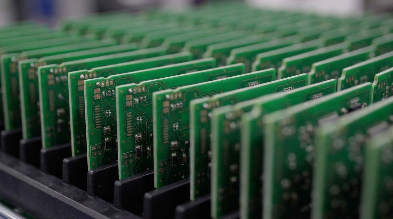
2. Copper Planes and Heavy Copper PCB Design for Heat Spreading
Thick copper planes spread heat laterally across PCB layers while also providing low-resistance current paths. Copper thicknesses of 2–6 oz significantly improve heat conduction and dissipation efficiency compared to standard 1 oz copper.
Large ground and power planes beneath heat sources act as efficient heat spreaders, and thermal vias move surface heat into internal planes for rapid lateral distribution. IPC-2152 standards define trace width requirements for a maximum 10–20°C temperature rise and factor in internal versus external layer placement and the presence of parallel heat-sinking planes.
3. Heat Sink Selection and PCB Integration
Heat sinks increase surface area for convective cooling and, when properly designed, can reach 2–4°C/W thermal resistance.
Heat sinks with 2°C/W thermal resistance manage 10 W components while keeping temperature rise below 20°C above ambient. Optimal fin spacing of 2–4mm maximizes surface area while promoting airflow. DFM considerations include placing heat sinks in unobstructed airflow regions and reserving mounting hole locations in the PCB layout to support repeatable assembly and long-term reliability.
4. Thermal Interface Materials (TIMs) for Reliable Contact
Thermal interface materials fill microscopic air gaps between components and heat sinks and remove the high thermal resistance of trapped air. TIMs with 1–3 W/m·K conductivity enhance heat sink performance, while materials exceeding 3 W/m·K conductivity provide stronger thermal coupling.
Phase-change materials and thermal pads conform to surface irregularities and maintain consistent contact over time. DFM guidelines define TIM thickness tolerances and application methods so that air bubbles and voids do not undermine thermal performance.
5. Metal-Core and Heavy Copper PCBs for High-Power Density
Aluminum-based PCBs offer 150–220 W/m·K thermal conductivity while copper-based PCBs reach 380–400 W/m·K, which dramatically outperforms standard FR-4 at 0.3–0.4 W/m·K.
Metal-core PCBs typically provide 1–3 W/m·K effective thermal conductivity for power electronics and other high-power applications. Advanced PCB materials introduce assembly challenges including thermal mass variation that affects reflow profiles and solder joint formation.
DFM protocols address these challenges through tuned reflow profiles, controlled preheat stages, and assembly processes that account for the higher thermal mass of metal-core and heavy copper substrates.
6. PCB Thermal Analysis Software and AI-Optimized Simulations
Engineers validate advanced material choices and layout strategies with thermal simulation before fabrication. Siemens EDA’s unified 3D IC thermal workflow reduces model build time from days to minutes using automated thermal model generation.
AI-assisted thermal analysis explores the design space by automatically generating and simulating thousands of model variants. AI now automates thermal analysis, component placement, routing, and design rule checks, which improves designs and shortens time-to-market.
Modern tools like ANSYS Icepak and Siemens Flotherm integrate with ECAD systems so teams can run thermal validation throughout the design phases instead of waiting for late-stage checks.
7. Direct Thermal Path Technology to Bypass PCB Resistance
Direct thermal path technology creates dedicated heat routes from high-power components to the chassis or external cooling hardware.
This proprietary approach bypasses traditional PCB thermal resistance by using direct metallic connections formed through specialized via structures and thermal bridges. Advanced implementations of this approach use copper-filled channels and thermal pillars that provide sub-1°C/W thermal resistance paths.
To make these high-performance thermal paths manufacturable, DFM integration ensures alignment with mechanical constraints and assembly processes while preserving electrical isolation where required.
8. Silver Sintering for High-Power Applications
Silver sintering delivers superior thermal and electrical performance compared to traditional solder joints and operates reliably above 200°C with about 30% lower thermal resistance than conventional attachment methods. This joining technology forms metallurgical bonds that maintain integrity under extreme thermal cycling and mechanical stress.
Silver-sintered joints show exceptional reliability in aerospace and defense applications where temperature excursions and vibration levels exceed solder capabilities. DFM considerations cover substrate preparation, sintering profile tuning, and in-process quality control to ensure consistent joint formation across production lots.
9. Conformal Coating in Thermal Extremes
Conformal coatings protect PCB assemblies during thermal cycling while still allowing effective heat dissipation. Advanced coating formulations add some thermal conductivity while guarding against moisture, contamination, and chemical exposure.
Environmental and stress testing, including thermal cycling, now occurs earlier in assembly processes to uncover latent defects. IPC and JEDEC standards guide coating selection and application methods for mission-critical hardware that must survive long-term exposure to temperature extremes.
10. Integrated Testing and Quality Control for Thermal Reliability
Comprehensive testing confirms thermal performance through automated optical inspection (AOI), thermal cycling, and functional verification. ANSYS Sherlock delivers first reliability analysis results in 1–3 days compared to 8–16 weeks for physical testing. Thermal imaging during functional testing reveals hotspots and validates simulation models.
Early defect detection through integrated testing prevents field failures and reduces warranty costs. DFM protocols also ensure test access and thermal sensor placement so teams can monitor temperatures in deployed systems over the product life.
PCB Thermal Management for Mission-Critical Industries
These ten techniques become especially critical in mission-critical industries where thermal failures can create safety risks and costly downtime. Aerospace and defense applications demand exceptional thermal reliability under vibration, temperature extremes, and long service cycles. AI servers’ increasing compute density forces PCB substrates to handle greater thermal stress and current density beyond 224 Gbps per lane toward 400 Gbps.
Pro-Active Engineering’s proprietary silver sintering and direct thermal path technologies address these challenges within AS9100 and ITAR-compliant processes. Advanced materials like metal-core boards and heavy copper layers are becoming more common for higher power densities, building on the heavy copper strategies discussed earlier.
DFM workflows combine IPC and JEDEC standards with 2026 trends such as 3D stacking architectures and advanced substrates. The thermal resistance formula θ = ΔT/P guides design optimization, where θ represents thermal resistance (°C/W), ΔT is temperature difference (°C), and P is power dissipation (W).
FAQ: PCB Thermal Management Engineering
What are the best PCB thermal via specifications for high-power applications?
Effective thermal vias typically use 0.3–0.5mm diameter with filled construction and at least 25μm copper plating thickness. Arrays should reach 200–400 vias/cm² density under high-power components and connect directly to large copper planes.
Filled vias provide about 30% better thermal performance than hollow vias and also prevent solder wicking during assembly. Staggered hexagonal patterns improve thermal transfer while keeping the design manufacturable.
How do I choose the right PCB thermal analysis software?
Thermal analysis software should integrate with ECAD tools and support AI-assisted optimization. Leading options include Siemens Flotherm, ANSYS Icepak, and Cadence Celsius.
Useful capabilities include automated model generation from design files, multi-physics coupling for combined thermal and structural analysis, and parametric optimization for design space exploration. AI-enabled solvers cut simulation time from days to minutes and improve accuracy through intelligent mesh creation and solver tuning.
What advantages does silver sintering offer over traditional attachment methods?
Silver sintering provides about 30% lower thermal resistance than solder joints while operating reliably above 200°C.
The metallurgical bond delivers higher mechanical strength under thermal cycling and vibration stress. Silver-sintered joints maintain electrical and thermal performance through temperature excursions that would degrade solder joints. As detailed in the silver sintering section, this capability supports aerospace and defense applications where reliability margins must remain high.
How does DFM integration reduce thermal design risks?
Early thermal simulation combined with DFM review cuts redesign cycles by 50–80% by exposing thermal bottlenecks before fabrication. Collaborative design reviews ensure manufacturing constraints stay visible during thermal design decisions.
Standardized thermal solutions and placement guidelines streamline production while preserving performance. Early prototype builds using production processes validate thermal models and reveal potential manufacturing issues before volume release.
What thermal management approaches work best for high-power regulated applications?
ITAR-regulated designs often rely on metal-core PCBs, advanced thermal interface materials, and rigorous testing protocols. The heavy copper construction discussed earlier, typically 2–6 oz, becomes essential when combined with filled thermal vias to spread heat efficiently.
Silver sintering technology supplies high-temperature attachment performance for mission-critical assemblies. Integrated testing that includes thermal cycling, vibration, and burn-in confirms long-term reliability under extreme operating conditions.
Partner with Pro-Active Engineering for Advanced Thermal Solutions
These ten advanced PCB thermal management techniques form a practical toolkit for reliable high-power electronics in mission-critical environments.
Pro-Active Engineering’s 30 years of experience, proprietary thermal technologies, and integrated DFM approach help teams avoid costly redesigns and reach first-pass success. The Speed Shop delivers thermal-optimized prototypes in 2–5 days using full production processes, and the ITAR-registered facility supports demanding aerospace and defense programs.
Transform your thermal challenges into competitive advantages with Pro-Active Engineering’s comprehensive thermal management solutions. Get started on your high-reliability project today.