Last updated: April 17, 2026
Key Takeaways for High-Power PCB Cooling
- Thermal via arrays with staggered hex patterns and filled conductive epoxy create efficient heat paths from components to internal planes, reducing hotspot temperatures.
- Heavy copper planes (2 oz and higher) spread heat and carry high current, enabling 70A per inch traces with only a 10°C rise in power electronics.
- Strategic component placement, multilayer thermal planes, and metal core PCBs with 120 to 237 W/m·K conductivity support extreme power densities without overheating.
- Advanced methods such as silver sintering, high-performance heat sink TIMs, and integrated cooling with vapor chambers or liquid systems lower junction-to-case thermal resistance.
- Pro-Active Engineering delivers 2 to 5 day ITAR-compliant prototypes with silver sintering and full thermal validation; get pricing for your production-ready high-power PCBs.
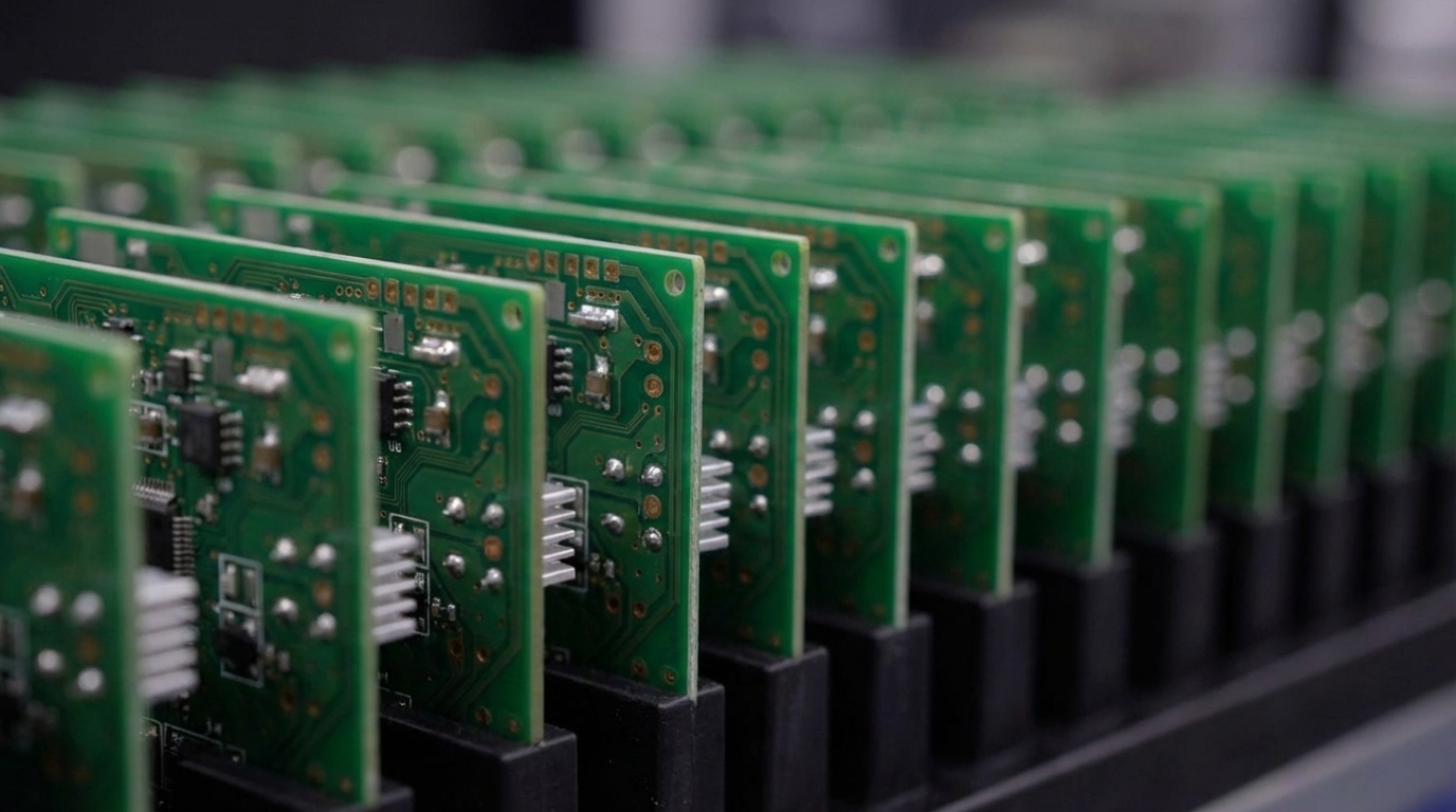
1. Thermal Via Arrays for Efficient Heat Transfer
Thermal via arrays create direct conduction paths from hot components to internal copper planes, forming the base of effective PCB heat dissipation. Staggered hex patterns increase via density and improve heat transfer across the component footprint. Via density directly affects thermal performance, with smaller diameters and tighter pitches supporting higher via counts and larger features offering a better cost and performance balance.
Critical design requirements start with appropriate thermal via pitch that prevents solder wicking during reflow. For manufacturing reliability, an aspect ratio of 10:1 ensures void-free copper electrodeposition in full wafer thickness through-silicon vias with tuned electrolyte and voltage parameters. Once vias are formed, filling them with conductive epoxy removes air gaps and increases thermal conductivity compared to plated-only designs. These vertical heat paths then work with horizontal heat spreading layers to create a complete thermal network.
2. Heavy Copper Planes for Horizontal Heat Spreading
Heavy copper layers spread heat horizontally and increase current-carrying capacity in high-power boards. A 2 oz external copper layer handles approximately 70 amps per inch of trace width at a 10°C temperature rise. In parallel, a solid ground plane serving as a heat spreader can reduce power MOSFET temperature by 15 to 20°C.
Design guidelines specify sufficient copper exposure in high-current regions to carry both electrical and thermal loads. Because copper width increases by approximately 0.0165% for every 10°C rise in ambient temperature, designers must account for thermal expansion in high-current traces. This requirement makes heavy copper construction valuable, since it provides direct thermal paths and enough cross-sectional area to support high current densities in power electronics.
3. Strategic Component Placement for Thermal Isolation
Component placement sets the stage for thermal isolation and hotspot control in high-power layouts. Placement should maintain adequate spacing between components to support heat dissipation and avoid shorts. Power devices need separation from temperature-sensitive circuits, and layout teams should define thermal zones early in the design.
Critical spacing guidelines use minimum clearances based on power dissipation levels, validated through thermal modeling to confirm safe temperatures. Components that generate more than 0.5 W require dedicated thermal management zones with direct via connections to heat-spreading planes. The 0.5 W threshold marks the point where passive air cooling alone often becomes insufficient for long-term reliability.
4. Heat Sink Integration and High-Performance TIMs
Heat sink integration converts board-level heat into system-level cooling, so mechanical and thermal design must align. Thermal relief spokes on through-hole pads prevent cold joints during soldering, and accurate land pattern design keeps mechanical attachment reliable under vibration and cycling.
Advanced thermal interface materials bridge the gap between components, PCBs, and heat sinks. Hybrid liquid metal TIMs that combine gallium alloys with solid components deliver very high thermal conductivity for applications exceeding 850 watts per die. These materials reduce interface resistance and support aggressive power densities when paired with well-designed sinks and planes.
5. Multilayer Thermal Planes and Embedded Heat Spreaders
Multilayer stackups with dedicated thermal planes create a three-dimensional heat dissipation network that complements via arrays and heat sinks. PCB layer stack-up should support thermal management with continuous power and ground planes that connect frequently to reduce impedance. At the same time, balanced copper distribution within 10% across layers and symmetric stackups lower delamination risk during thermal cycling.
Embedded thermal structures such as copper-filled channels and integrated heat spreaders add direct conduction paths inside the board. These features move heat away from hotspots while preserving electrical isolation where needed, and they work best when aligned with component placement and via fields.
6. Metal Core PCBs for Extreme Power Densities
Metal Core PCBs (MCPCBs) support power levels that exceed standard FR-4 capability. Aluminum substrate materials in aluminum PCBs provide thermal conductivity around 237 W/m·K for pure aluminum and 120 to 220 W/m·K for alloys. Copper-core PCBs offer even higher conductivity, and both options outperform standard FR-4 at roughly 0.3 W/m·K.
MCPCBs improve vertical heat dissipation when designers combine them with thermal vias and heavy copper planes. These substrates also show better reliability than FR-4 in demanding temperature environments, especially when paired with advanced attachment methods that minimize interface resistance.
7. Silver Sintering and Low-Resistance Thermal Interfaces
Silver sintering delivers one of the lowest thermal resistance attachment methods for mission-critical power electronics. This process creates a thin, highly conductive bond line that outperforms traditional solder joints in junction-to-case thermal resistance. The resulting interfaces maintain strength and conductivity at elevated temperatures, which supports long-life operation under thermal cycling.
Pro-Active Engineering uses silver sintering to form direct thermal paths that remove bottlenecks between high-power components and their substrates, including MCPCBs. These assemblies support higher power densities while preserving reliability in aerospace and defense programs. Contact our thermal engineering team for silver-sintered assemblies that meet mission-critical requirements.
8. Advanced Thermal Simulation and Design Validation
Advanced thermal simulation guides every earlier design choice, from via arrays to cooling hardware. Modern tools predict hotspots and allow engineers to refine layouts before fabrication. Leaf-vein-inspired fractal microchannels can significantly reduce maximum junction temperature when optimized with FEM-based methods, and Fourier series-based thermal modeling can run faster than traditional FEM while maintaining accuracy.
Validation then confirms that simulated performance holds in real hardware. Comprehensive thermal cycling tests and infrared imaging verify model accuracy, and hotspots must remain below the substrate glass transition temperature (Tg). Tools such as ANSYS Icepak and FloTHERM support this workflow by linking detailed models with measured results.
9. Conformal Coatings that Protect Without Trapping Heat
Conformal coatings protect high-power boards from harsh environments while still allowing heat to escape. Advanced formulations increase thermal conductivity and shield against moisture, contamination, and thermal cycling stress. Selection focuses on balancing thermal performance with the required level of environmental protection.
Application methods must control coating thickness carefully so the film does not act as unwanted insulation. Consistent coverage over critical thermal paths and components preserves both cooling performance and long-term reliability.
10. Integrated Cooling with Heat Pipes, Vapor Chambers, and Liquid
Integrated cooling solutions handle the highest power densities by combining the PCB with system-level hardware. Embedded heat pipes, vapor chambers, and liquid cooling interfaces move large amounts of heat away from the board. Future AI server PCBs already include interfaces for cold plates and microchannel liquid cooling systems as liquid cooling becomes mainstream.
Design teams must coordinate mechanical integration, fluid routing, and fail-safe operation when they add active cooling. Smart PCBs use embedded temperature sensors and thermal expansion control structures for real-time monitoring. These features close the loop between simulation, hardware, and system controls.
Validating Thermal Strategies in Mission-Critical Hardware
Robust thermal validation combines simulation, testing, and standards-based qualification. Reliability verification includes thermal cycling from -40°C to 125°C under ASTM D149 and compliance with IPC-6012 for rigid PCB performance. Advanced simulation tools support optimization of complex geometries, and multi-objective genetic algorithms can improve heat transfer coefficients while respecting pressure limits.
Mission-critical programs highlight the value of integrated thermal design that spans layout, materials, and assembly. Defense and aerospace projects require thermal modeling that optimizes layer count, copper distribution, via density, and component placement. Pro-Active Engineering’s ITAR-compliant processes keep these strategies consistent from prototype through production.
Offshore EMS vs. Integrated US Thermal Partners
Manufacturing partner choice directly affects thermal performance, schedule, and risk. Thermal management success depends on both technical capability and how tightly design, fabrication, and assembly stay integrated. The table below shows a key tradeoff: offshore providers offer basic thermal features with longer timelines and higher IP risk, while integrated US partners such as Pro-Active deliver advanced techniques like silver sintering with roughly 20% lower total cost of ownership despite higher unit prices.
| Provider Type | Lead Times | Thermal Expertise | Compliance/TCO |
|---|---|---|---|
| Offshore EMS | 8-12 weeks | Basic vias/planes | IP risk, high rework |
| Large EMS | 4-6 weeks | Generic MCPCBs | Volume-focused, no ITAR |
| Pro-Active | 2-5 days | Silver sintering | ITAR/AS9100, 20% lower TCO |
For high-power boards that depend on advanced thermal management, Pro-Active Engineering’s integrated workflow keeps design intent aligned with manufacturing reality. Start your rapid thermal prototype with our 2 to 5 day Speed Shop service using production-ready processes.
Frequently Asked Questions
What thermal via sizing provides optimal heat transfer for high-power components?
Beyond diameter and pitch, via placement pattern strongly affects heat transfer. Staggered hex arrays often outperform simple grid patterns by 15 to 20% because they distribute heat more uniformly under the component footprint. Filled vias with conductive epoxy still provide the best conduction path by removing air gaps and improving contact to internal planes.
Which thermal simulation software provides the most accurate hotspot prediction?
ANSYS Icepak and FloTHERM provide leading hotspot prediction accuracy for PCB applications. Advanced Fourier series-based modeling can shorten computation time compared to traditional FEM while preserving precision. Multi-objective genetic algorithms combined with 3D conjugate heat transfer simulations help optimize complex thermal geometries under real operating constraints.
How do DFM principles ensure thermal reliability in manufacturing?
DFM for thermal reliability focuses on consistent copper thickness, robust solder joints, and stable stackups. Key guidelines include maintaining copper thickness tolerances to avoid unexpected temperature rise, using thermal relief spokes on high-power pads, and keeping via aspect ratios within limits that support void-free plating. Balanced copper distribution across layers prevents delamination during thermal cycling, and proper component spacing preserves airflow and conduction paths.
What lead times can Pro-Active Engineering achieve for thermal prototypes?
Pro-Active Engineering’s Speed Shop delivers thermal-focused prototypes in 2 to 5 days using full production processes. This rapid service includes thermal via arrays, heavy copper layers, and advanced materials such as silver sintering so prototype performance matches production behavior without late-stage thermal surprises.
How does thermal design scale from prototype to ITAR production?
Pro-Active Engineering maintains consistent thermal performance from early prototypes through ITAR-compliant production by using the same qualified processes and materials. Silver sintering, controlled copper thickness tolerances, and comprehensive thermal validation support mission-critical reliability. AS9100 and ITAR certifications provide secure scaling for defense and aerospace programs.
Secure Thermal Reliability in High-Power Designs
These ten thermal management strategies work together as a complete toolkit for high-power PCB challenges. Optimized via arrays, heavy copper planes, MCPCBs, advanced attachment methods, and integrated cooling each address specific thermal bottlenecks while supporting DFM and reliability requirements. Success depends on aligning design, simulation, materials, and manufacturing under one coordinated approach.
Partner with Pro-Active Engineering for mission-critical thermal success. Our silver sintering technology, 2 to 5 day prototyping, and ITAR-compliant production keep your thermal strategies performing as modeled. Request a quote today for thermal-optimized PCBs that avoid late-stage surprises and deliver reliable performance in demanding applications.