Last updated: April 17, 2026
Key Takeaways
- Limit flex PCB bends to 90° with static radii of 6-10x thickness and dynamic up to 100x thickness to reduce trace cracking from mechanical stress.
- Position vias at least 1.5 mm from bend zones, use teardrop pads, and route traces perpendicular to the bend axis for consistent stress distribution.
- Select adhesiveless polyimide with rolled annealed copper and keep components on rigid sections only to support long-term flex endurance.
- Follow IPC-2223 standards for trace width, spacing, and bend ratios, then confirm performance through prototype reliability testing in high-rel applications.
- Pro-Active Engineering’s Speed Shop offers 2-5 day prototyping and free DFM review to reduce failures, so request a quote today for a smooth transition into production.
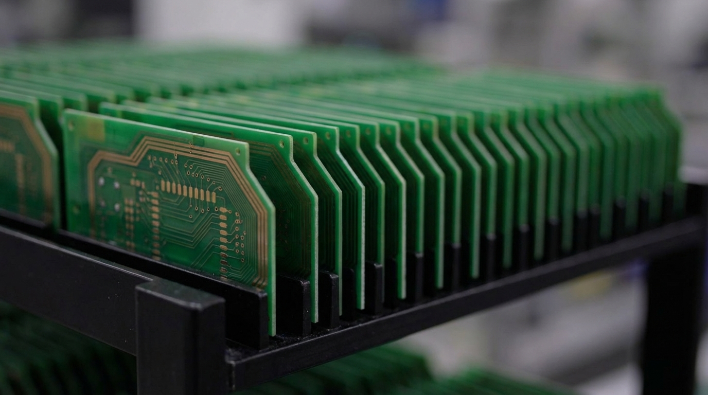
Essential DFM Rules for Flex PCB Reliability
These ten core rules address the most common flexible PCB failure modes in aerospace and defense programs. Applying them early in layout prevents expensive redesigns later.
1. Minimize bend angles: Limit bends to a maximum of 90° to reduce copper stress and prevent trace cracking during installation and operation.
2. Follow bend radius guidelines: Follow IPC-2223 bend radius guidance, which varies by layer count and application type. Static applications typically use 6-12x board thickness, while dynamic applications can require 20-200x thickness depending on configuration.
3. Keep vias away from bend zones: Position vias at least 1.5 mm from rigid-to-flex transitions to avoid stress concentration and cracking around plated holes.
4. Use teardrop pads: Add copper fillets at trace-to-pad junctions to spread stress and reduce pad lifting or trace necking during flexing.
5. Route perpendicular to bend axis: Run traces perpendicular to bend lines so the copper stretches evenly instead of concentrating strain along the trace length.
6. Implement strain relief: Add loops, curves, or serpentine routing in flex regions to absorb mechanical stress and extend flex life in dynamic applications.
7. Keep components off flex areas: Place all components on rigid sections to avoid solder joint fatigue and mechanical damage during bending.
8. Use appropriate materials: Polyimide films like Kapton® provide stable performance through repeated bending and high temperatures, which supports high-reliability designs.
9. Use adhesiveless construction: Adhesiveless laminates remove crack-prone adhesive layers and enable thinner, more reliable stackups.
10. Ensure IPC-2223 compliance: Follow industry standards for trace width, spacing, materials, and bend ratios to maintain manufacturability and predictable reliability.
Speed Shop prototyping validates these rules with the same rigorous testing used for production, so your design survives real operating conditions before full-scale build.
Flex PCB Bend Radius and Routing Guidelines
Among the ten rules above, bend radius choices have a direct impact on long-term reliability. The following table shows how bend radius requirements scale with layer count and application type, with dynamic designs needing larger radii to prevent fatigue failures.
| Application Type | Copper Weight | Static Radius | Dynamic Radius |
|---|---|---|---|
| Single-layer | 0.5 oz (18 μm) | 3-6x thickness | 20-40x thickness |
| Double-layer | 0.5 oz (18 μm) | 6-10x thickness | 20x-100x thickness |
| Multilayer (4L+) | 0.33 oz (12 μm) | 10-15x thickness | 10x minimum |
Use curved or serpentine routing perpendicular to bend directions and replace solid copper planes with hatched copper patterns in flex regions. Hatched patterns maintain flexibility while still providing shielding. Pro-Active Engineering’s HDI layout experience helps prevent fatigue failures in defense hardware exposed to severe vibration and thermal cycling.
Vias, Pads, and Stress Relief in Flexible Layouts
Via placement represents the primary failure mode in flexible PCBs. Vias on bend lines cause the number one field failure in rigid-flex designs. As noted in the design rules, maintain spacing from transitions, then add via tenting and stagger vias across layers to reduce stress concentration. Use only the minimum number of vias in flex areas and maintain sufficient annular rings when placement cannot move.
Teardrop pads and anchor spurs under coverlay help keep pads attached and prevent trace separation during repeated flexing. Add strain relief features such as slots, fillets, or smooth curved transitions at rigid-to-flex boundaries to soften stress gradients. Consistent DFM practice improves production yield and lowers field failure rates in Class 3 applications.
Pro-Active Engineering’s 100% AOI and flying probe testing in Speed Shop prototypes identifies these issues early, which prevents costly redesigns during production. Request a 2-5 day prototype quote to confirm your via and pad strategy before release.
Stackup, Materials, and Component Placement Choices
Material selection and copper weight must match the flex behavior your application requires. The table below maps typical stackups to suitable use cases so you can align your design with the right construction.
| Layer Count | Material | Copper Weight | Application |
|---|---|---|---|
| 2-layer | Adhesiveless polyimide | 0.5 oz RA copper | Dynamic flex |
| 4-layer | Polyimide with coverlay | 0.33 oz RA copper | High-density static |
| 6-layer+ | Rigid-flex hybrid | 1 oz ED copper (rigid only) | Complex systems |
Avoid SMD components in bend areas and use flexible adhesives for stiffener attachment to prevent peeling. FR-4 or thick polyimide stiffeners near connectors move bend points away from solder joints and reduce fatigue. Rolled annealed copper with its ductile grain structure resists cracking under repeated bending more effectively than electrodeposited copper.
Pro-Active Engineering’s thermal-optimized layouts, which use silver sintering and direct thermal path techniques, support reliable performance in high-power aerospace assemblies.
IPC-2223 Standards and High-Rel Considerations
IPC-2223 recommends minimum bend radii of 100:1 for single-layer, 150:1 for double-layer, and up to 200:1 for multilayer dynamic flex circuits and specifies minimum bend radius ratios of 6:1 for single-layer, 12:1 for double-layer, and 24:1 for multilayer static flex applications, where the radius equals the ratio multiplied by the total thickness of the flexible portion, along with copper adhesion requirements. IPC-TM-650 defines dynamic bending tests that quantify flex endurance.
High-reliability applications require additional safeguards beyond baseline IPC rules. ITAR and defense programs need enhanced vibration resistance for launch and flight, thermal cycling capability for wide temperature swings, and secure manufacturing processes that protect sensitive designs. These needs call for specialized certifications. Pro-Active Engineering’s Nadcap accreditation validates advanced process control, while AS9100 certification confirms aerospace-grade quality systems that many generic manufacturers lack.
9-Point DFM Checklist for Flex PCB Layouts
This checklist summarizes when and how to apply the guidelines above during layout. Use it during early design reviews and again before releasing fabrication files.
• Conduct pre-layout DFM review with your manufacturing partner
• Plan bend locations and calculate minimum radii
• Position vias away from flex zones and transitions
• Route traces perpendicular to bend axis with smooth curves
• Select materials that match electrical, thermal, and flex requirements
• Design stackup for both thermal and mechanical performance
• Add strain relief at critical stress points
• Verify IPC-2223 compliance for all specifications
• Collaborate on Gerber review with Pro-Active engineers
Pro-Active Engineering’s integrated DFM process identifies reliability risks before fabrication, which reduces prototype-to-production disconnects that often appear with traditional contract manufacturers.
A recent aerospace customer achieved zero failures in 100,000 flex cycles and thermal testing through Pro-Active’s Speed Shop iteration process. The 3-day prototype turnaround enabled rapid design refinement that would have taken weeks with offshore suppliers, demonstrating the value of tightly integrated engineering and manufacturing.
Conclusion
Reliable flexible PCB layouts depend on proven DFM practices that cover bend radius choices, material selection, trace routing, and via placement. These rules reduce fatigue failures that can cost aerospace and defense programs millions in redesigns and schedule slips. Pro-Active Engineering’s 30+ years of high-reliability experience, combined with Speed Shop rapid prototyping and ITAR-compliant manufacturing, help your flexible PCB designs meet mission-critical requirements from concept through production. Request a free DFM review or 2-5 day prototype quote today to avoid manufacturing surprises and accelerate your program timeline.
Common Flex PCB DFM Pitfalls That Cause Failures
Vias placed on bend lines represent the number one cause of field failures in flexible PCBs. The rigid plated hole creates a stress concentration point that cracks under repeated flexing. Other frequent pitfalls include insufficient bend radius that overstretches copper, solid copper planes in flex areas that restrict movement, components mounted in bend zones that drive solder joint failures, and missing strain relief at rigid-to-flex transitions. Sharp trace angles and unsuitable material choices also shorten life in high-reliability applications.
DFM Differences Between Rigid-Flex and Pure Flex Circuits
Rigid-flex PCBs require extra attention at rigid-to-flex transition zones where different materials and thicknesses create stress concentration points. These transitions need larger keepout zones for vias and components, specialized adhesive systems to bond dissimilar materials, and careful stackup design to manage thermal expansion differences. Pure flex circuits distribute stress more uniformly but rely on consistent material properties across the entire design. Rigid-flex assemblies also need stiffeners under connectors and components, while pure flex circuits usually avoid components in bend regions altogether.
Bend Radius Targets for Aerospace Designs With 10,000+ Flex Cycles
Dynamic aerospace applications that require more than 10,000 flex cycles typically use bend radii of 20-100x the total flex thickness, depending on configuration and reliability margin. Single-layer designs can use the lower end of this range, while multilayer constructions need larger radii. Use rolled annealed copper at 0.5 oz or thinner, adhesiveless polyimide construction, and limit the flex region to two layers maximum. Validate the final radius through prototype testing that reproduces the operating environment and cycle count.
Material Choices for High-Temperature Flex PCB Reliability
Polyimide materials like Kapton offer thermal stability up to 400°C compared to PET, which has a maximum continuous thermal stability of 150°C (short-term up to 180°C) for flex PCBs or PEN at roughly 180-200°C, so polyimide suits aerospace and defense environments. The material choice affects temperature tolerance and mechanical fatigue resistance, with polyimide maintaining flexibility and electrical properties through thousands of bend cycles. Coverlay selection also matters, with acrylic adhesives providing better flexibility than many epoxy systems. Advanced materials such as self-healing polymers and liquid metal traces are emerging for extreme reliability but require specialized manufacturing processes.
Testing Required to Validate Flex PCB DFM Before Production
Comprehensive flex PCB validation includes mechanical bend testing to the specified cycle count and radius, thermal cycling across operating extremes, vibration testing per aerospace specifications, and electrical continuity monitoring during all tests. Prototype evaluation should also include accelerated aging, humidity exposure, and mechanical shock to simulate field conditions. Visual inspection for trace cracking, delamination, and coverlay damage provides early indicators of weakness. Pro-Active Engineering’s Speed Shop supports rapid iteration of these tests within a few days so you can refine the design before committing to production tooling.