Last updated: April 17, 2026
Key Takeaways
- Maximize copper plane coverage to 80-90% and use 2-3oz heavy copper weights to spread heat laterally and reduce hotspots.
- Deploy thermal via stitching arrays with 0.3-0.5mm diameters at 1-2mm pitch, and enhance them with filled vias and via-in-pad designs for efficient interlayer heat transfer.
- Balance copper distribution across symmetric layers and integrate power and ground planes to prevent warpage while creating parallel thermal paths that can reduce hotspots by about 15°C.
- Position heavy copper on inner layers, run simulations with ANSYS or Flotherm using IPC-2152 guidance, and confirm results with rapid prototyping to ensure manufacturable thermal performance.
- Pro-Active Engineering delivers ITAR and AS9100 compliant heavy copper PCBs with silver sintering and rapid Speed Shop prototyping; request a quote to discuss your thermal management requirements.
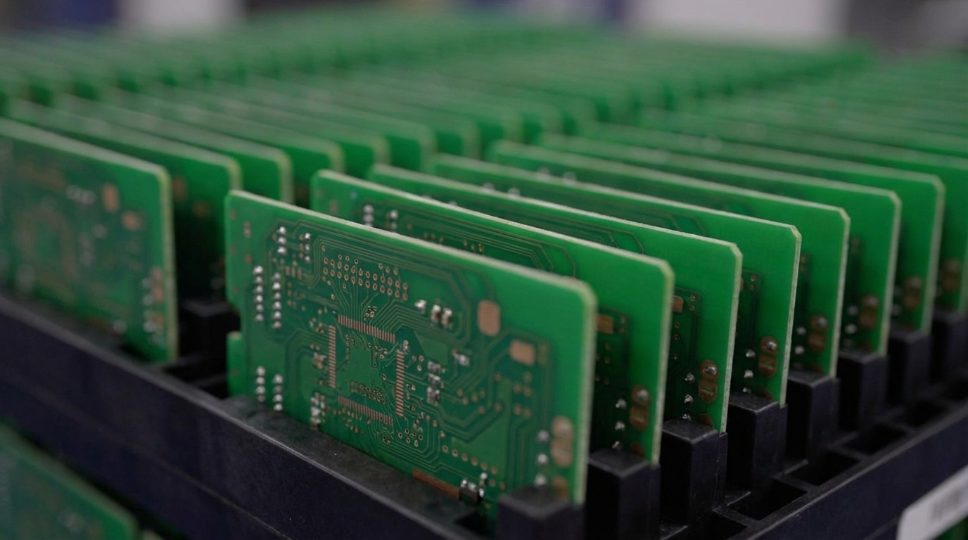
10 Best Practices for Copper Planes in PCB Thermal Management
1. Maximize Plane Coverage for Strong Lateral Heat Spreading
Maintain 80-90% copper fill across plane layers to improve lateral heat spreading. This high coverage keeps heat flowing through wide, low-resistance paths instead of narrow constrictions. Gaps larger than 1mm create thermal bottlenecks that force heat through smaller regions and raise local temperatures. Large continuous copper areas provide the lowest thermal resistance paths from heat sources to cooling mechanisms. However, excessive copper coverage without proper balancing can cause warpage, so staying near the 80-90% range avoids mechanical issues. Pro-Active's DFM review identifies practical coverage ratios during the design phase and prevents manufacturing problems before they appear.
2. Select Heavy Copper Weights for Higher Current and Lower ΔT
Use 2-3oz copper for improved temperature performance in high-power applications. 2oz finished copper provides improved heat dissipation for medium-power electronics, while 3oz copper offers excellent thermal dissipation for high-power electronics. The following table shows how copper weight affects thickness, temperature reduction, and current capacity so you can match copper weight to your power and thermal requirements:
| Copper Weight | Thickness (µm) | ΔT Reduction | Current Capacity (A) |
|---|---|---|---|
| 1oz | 35 | Baseline | Low |
| 2oz | 70 | Improved | Medium |
| 3oz | 105 | Further improved | Higher |
DFM consideration: Heavy copper at or above 3oz needs appropriate etching tolerances and increased spacing to maintain reliable production yields.
3. Implement Thermal Via Stitching Arrays for Vertical Heat Flow
Deploy 0.3-0.5mm diameter vias at 1-2mm pitch to create efficient heat transfer paths between layers. These via arrays move heat vertically from hot components into internal planes and heat-spreading layers. The table below compares three common via configurations and highlights how smaller diameters and tighter pitch improve thermal performance but increase manufacturing cost and complexity:
| Via Diameter (mm) | Pitch (mm) | Density (vias/cm²) | Performance |
|---|---|---|---|
| 0.3 | 1.0 | High | Highest |
| 0.4 | 1.2 | Medium | Good balance |
| 0.5 | 1.5 | Lower | Cost-effective |
Pro-Active's silver sintering technology increases via thermal conductivity beyond standard plating methods and supports demanding power densities. Request a quote to explore how silver sintering can enhance your thermal via design.
4. Use Via-in-Pad with Thermal Reliefs for Solder Control
Implement spoke patterns for thermal reliefs to prevent solder wicking while still maintaining strong thermal conductivity. IPC-4761 Type VII filled and capped vias prevent solder wicking and ensure pad flatness. These filled vias support reliable assembly on power pads and fine-pitch components. Connect thermal vias directly to solid copper planes without relief patterns when you need maximum heat transfer efficiency from high-power devices.
5. Balance Copper Distribution to Control Warpage
Maintain symmetric copper pours to prevent warpage. When one layer carries much more copper than the opposite layer, differential thermal expansion during reflow bends the board and creates bow or twist. Industry standards limit maximum acceptable PCB warpage to protect assembly reliability and solder joint quality. Maintain similar copper coverage across layers and use dummy fills in low-copper areas to balance the copper distribution and keep the stackup mechanically stable.
6. Integrate Power and Ground Planes for Parallel Thermal Paths
Combine power and ground planes for dual heat spreading that can reduce hotspots by about 15°C. Multiple plane layers create parallel thermal paths that share the heat load and lower temperature rise around high-power components. These planes also improve current distribution and reduce voltage drop across the board. Design planes with minimal splits so heat and current can flow across continuous copper surfaces. Pro-Active's multilayer expertise supports plane integration that meets both thermal and electrical performance targets.
7. Optimize Plane Thickness Layering After Plane Assignment
Position heavy copper planes on inner layers for maximum thermal mass without surface constraints. Inner layers allow thicker copper weights than outer layers, where surface mount pad geometry and fine-pitch routing limit copper thickness. This thickness advantage reduces thermal resistance and moves heat more quickly toward cooling mechanisms. Buried planes also provide density benefits and help you meet overall board thickness targets while still using heavy copper where it matters most.
8. Add Filled Vias and Microvias for Dense Thermal Paths
Use conductive fill for superior thermal performance in high-density designs. Filled thermal vias using conductive epoxy or copper provide superior thermal performance compared to plated-only vias. Conductive fill increases the effective cross-sectional area for heat flow and improves reliability in stacked or staggered via structures. Maintain appropriate aspect ratios so plating quality and thermal conductivity remain consistent across the entire via field.
9. Simulate Thermal Performance Before Finalizing Layout
Validate designs using ANSYS or Flotherm before layout completion to identify hotspots and refine plane placement. Follow IPC-2152 standards for current calculations and thermal modeling so trace and plane temperatures stay within safe limits. Early simulation confirms that selected copper weights, via configurations, and plane locations can meet thermal targets. This early insight avoids costly redesigns and schedule slips later in the development cycle.
10. Validate Thermal Design with Rapid Prototyping
Test thermal performance with production-ready prototypes that use AOI and functional testing. Pro-Active's Speed Shop delivers prototypes in 2-5 days using full production processes, so thermal behavior in prototypes matches behavior in volume builds. Thermal imaging and junction temperature measurements confirm simulation results and highlight any remaining hotspots before you commit to production tooling.
DFM Checklist and Common Pitfalls for Manufacturable Copper Planes
Essential DFM Requirements:
- Adequate thermal via pitch to prevent solder wicking
- Appropriate thickness tolerance for copper at or above 3oz with suitable minimum spacing
- Balanced copper coverage across layers
- Thermal relief spoke patterns for assembly reliability
- Symmetric stackup design for warpage control
Common Pitfalls: Warpage in high-density boards from unbalanced copper distribution, late-stage thermal discoveries that force redesigns, and insufficient via plating thickness that reduces thermal conductivity often appear together in heavy copper projects. Pro-Active's integrated DFM review identifies these risks during the design phase, prevents production delays, and supports first-pass success.
Why Pro-Active Engineering Excels in Copper Plane Thermal Solutions
With more than 30 years of PCB experience, Pro-Active Engineering delivers advanced thermal management through silver sintering, direct thermal paths, and heavy copper capabilities. Our Speed Shop provides production-ready prototypes using full manufacturing processes, which keeps design-to-production transitions smooth and predictable. ITAR registration, AS9100 certification, and Nadcap accreditation support mission-critical applications in defense and aerospace programs.
Case example: Pro-Active's silver sintering and optimized thermal via arrays reduced hotspots by 25% in an aerospace power module, extended component life, and improved overall system reliability. This integrated engineering approach removes the prototype-to-production disconnects that often slow down traditional manufacturing partnerships.
Contact our engineering team to discuss thermal management solutions for your next high-power PCB project.
Frequently Asked Questions
What copper weight reduces hotspots by 20°C in high-power PCBs?
Thicker inner copper layers can provide significant temperature reduction compared to 1oz copper and help reduce hotspots in high-power applications. The exact reduction depends on component power density, board layout, and cooling system design. For applications that need higher thermal performance than 2oz copper can provide, 3oz copper offers additional benefits, while 4oz and higher copper weights support specialized high-current applications where maximum conductivity is essential.
What is the optimal thermal via pitch for maximum heat transfer?
Pitch in the 1.0-1.5mm range with 0.3mm diameter vias provides a strong balance of thermal performance and manufacturing reliability. Closer spacing increases via density and improves heat transfer but raises the risk of solder wicking during assembly. Wider spacing lowers via count and reduces thermal effectiveness. The best configuration depends on component thermal pad size, power dissipation level, and assembly requirements, and dense via arrays can handle demanding power device thermal loads.
What warpage limit ensures reliable assembly with heavy copper PCBs?
Maintaining warpage within acceptable limits, measured as maximum deviation divided by board diagonal length, supports reliable SMT assembly. Heavy copper boards need careful copper balancing across layers and symmetric stackup design to avoid thermal expansion mismatches. Boards with excessive warpage experience component placement issues, solder joint reliability problems, and higher assembly defect rates, especially with fine-pitch components.
What DFM considerations apply to 3oz and heavier copper designs?
Heavy copper designs require etching tolerance accommodation, increased trace width and spacing, appropriate via pitch, and careful copper balancing to prevent warpage. Etching precision decreases as copper thickness increases, so wider traces and spacing improve yield. Drilling through heavy copper accelerates tool wear and can affect via quality. Early DFM review highlights these constraints and adjusts the design for consistent production success.
How quickly can Pro-Active deliver thermal-optimized prototypes?
Pro-Active's Speed Shop delivers production-ready prototypes in 2-5 days using full manufacturing processes that include heavy copper, thermal vias, and advanced interconnect technologies. All prototypes maintain ITAR compliance and receive comprehensive testing to validate thermal performance. This rapid turnaround supports iterative design refinement while still meeting schedule commitments for mission-critical programs.