Last updated: April 17, 2026
Introduction
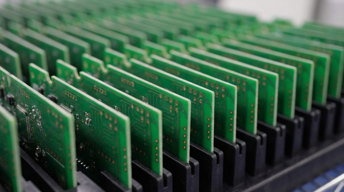
High-power electronics in aerospace and defense systems generate significant heat inside compact 6-layer PCBs. Poor thermal design can trigger intermittent faults, shorten component life, and jeopardize mission success. This guide walks through practical thermal design practices that keep 6-layer boards stable across wide temperature ranges.
Key Takeaways
- Use 6-layer stackups with thick copper inner planes and high-Tg FR4 for strong thermal spreading and stable signal integrity.
- Deploy dense thermal via arrays (0.2-0.3mm, 10-20 vias/cm², filled and capped) tied directly to copper planes without thermal reliefs.
- Combine heavy copper planes and widened traces (for example, 2.78mm for 5A) with I²R calculations to carry high current without hotspots.
- Place high-power components near board edges and along airflow paths, with even distribution and thermal isolation for sensitive circuits.
- Pro-Active Engineering provides DFM-focused thermal design support, rapid 2-5 day prototyping, and AS9100/ITAR-certified production; get a custom stackup review to validate your thermal approach.
Core Best Practices Summary
Effective thermal management in 6-layer high-reliability PCBs relies on a coordinated strategy. Designers must address board structure, heat transfer paths, and component-level behavior as a single system. Six essential practices work together to create a complete thermal solution:
- Optimize the 6-layer stackup with thick copper on inner planes.
- Deploy dense thermal via arrays as detailed below.
- Use thick copper for power planes with appropriate trace widths based on I²R calculations.
- Place high-power components near edges and convection paths with even distribution.
- Select high-Tg materials and appropriate thermal interface materials.
- Simulate and validate thermal performance using ANSYS or Flotherm plus IR imaging.
The following sections examine each practice in detail, starting with the foundation of thermal design: stackup optimization.
Thermal-Focused 6-Layer Stackup Design
Asymmetric stackups improve thermal spreading through deliberate copper placement. This structure positions thick copper planes close to high-power components while preserving signal integrity and controlled impedance.
The following specifications define a thermal-focused 6-layer stackup that balances heat spreading with signal performance:
- Signal L1 and L6 using 1oz standard copper
- Thick inner planes dedicated to heat spreading and power distribution
- High-Tg FR4 for stable performance at elevated temperatures
- Via-in-pad capability for direct thermal coupling under power packages
- Buried plane connectivity that supports lateral heat spreading across the board
WonderfulPCB’s Type 1 stackup provides extensive copper mass for heat spreading through adjacent ground and power planes that also create strong decoupling capacitance. This structure supports stable operation in high-power scenarios where both noise and temperature margins are tight. Pro-Active Engineering’s DFM reviews confirm that stackups meet thermal and manufacturability targets before layout proceeds.
Thermal Via Arrays for Reliable Heat Transfer
NextPCB recommends 0.2–0.4 mm diameter thermal vias with 10-20 vias/cm² under ICs, filled and capped per industry standards for vibration resistance. Optimal thermal via pitch is 0.635 mm using 0.25 mm drills, which balances copper density with mechanical strength.
High-reliability via design focuses on three main risks: solder wicking, thermal resistance, and plating defects. Filled and capped construction prevents solder wicking into via barrels during reflow. Direct connection to solid copper planes, without thermal reliefs, lowers thermal resistance between components and inner planes. Aspect ratios at or below 10:1 support uniform plating and reduce the chance of barrel cracks during thermal cycling.
Package-level details also matter. Grid patterns under QFN and BGA thermal pads increase contact area and improve vertical heat transfer into the board. Minimum spacing of 0.2mm between vias prevents antipad overlap that could weaken the dielectric or compromise isolation. Together, these practices create robust thermal pathways that survive harsh environments.
Pro-Active Engineering’s precision via technology maintains consistent thermal performance in high-reliability assemblies. Controlled drilling, plating, and filling processes meet IPC Class 3 requirements while preserving via integrity through repeated thermal cycles.
Copper Planes, Thickness, and Trace Routing for Heat
ALLPCB states that a power plane with a copper thickness of 1 oz/ft² can handle currents up to 10A with minimal loss when designers use full copper pours and teardrops. Copper foils carry current according to IPC-2152 guidelines, and 100 mil wide traces handle about 10A on outer layers with 1 oz copper per standard trace width rules.
Thermal copper design starts with thick copper on power planes to increase heat spreading capacity. This base allows wider traces sized for their current loads so that I²R heating stays within acceptable limits. Designers verify performance through ΔT = I²R / k calculations for worst-case operating conditions. Maximizing copper coverage through full plane pours, tied together with via stitching, creates continuous thermal paths that move heat away from hotspots.
Pro-Active Engineering supports heavy copper implementations for energy and high-current applications. Advanced manufacturing processes maintain dimensional stability and reliability while increasing current capacity and thermal spreading.
Component Placement Strategies to Reduce Hotspots
NextPCB advises spreading high-power components evenly across PCBs with 1.5x height spacing and close proximity to ground planes. Strategic placement near board edges uses natural convection while still meeting vibration and mechanical constraints for high-reliability systems.
Effective placement prevents hotspots through even distribution of power devices across the board area, which avoids concentrating heat in a single region. Aligning high-power components with airflow paths supports convection cooling and improves fan efficiency. Shorter components placed upstream keep airflow clear for taller parts downstream, which often run hotter.
Locating heat-generating components near board edges helps heat escape into the surrounding environment instead of remaining trapped in the center of the PCB. Thermally isolating sensitive circuits, such as precision analog or RF sections, limits heat transfer from nearby power components. Together, these placement choices reduce peak temperatures and improve long-term reliability.
Component placement determines where heat originates on the board, while material selection determines how effectively that heat moves through the stackup and out of the assembly.
Advanced Materials and Thermal Interfaces
High-Tg FR4 materials with Tg ≥170°C provide superior thermal stability and resist delamination during lead-free soldering with peak reflow temperatures up to 260°C. Materials such as Rogers 4350B and similar laminates add higher thermal conductivity for extreme environments and RF-heavy designs.
Pro-Active Engineering’s proprietary silver sintering technology delivers higher thermal conductivity than traditional solder joints. This process creates direct, low-resistance thermal paths between components and copper, which benefits mission-critical applications that run near their thermal limits. The advanced material portfolio includes thermal interface materials with k values above 5 W/mK and specialized substrates tailored for aerospace and defense requirements.
Consult with our materials engineers to select the most suitable thermal substrate and interface stack for your application.
Simulation, Validation, and Rapid Prototyping
ANSYS and Flotherm simulations define acceptable temperature rise early in the design process. Engineers then confirm these predictions through IR imaging and thermocouple measurements on production-ready prototypes. Pro-Active Engineering’s Speed Shop delivers 2-5 day prototyping with 100% AOI and functional testing so thermal performance can be verified before full production.
Our integrated workflow includes:
- Thermal modeling with component-level accuracy
- Rapid prototype validation using the same processes as production
- IR imaging to identify hotspots and confirm model accuracy
- Iterative design refinement based on measured data
- Production transfer with no gaps between prototype and volume builds
These simulation and validation practices proved critical in a recent aerospace application that pushed the limits of 6-layer thermal design.
High-Rel Case Study: Aerospace/Defense 6-Layer Success
A recent aerospace project required thermal control for a high-power CPU on a 6-layer board operating from -55°C to 125°C. Pro-Active Engineering’s silver sintering approach reduced hotspot temperatures compared to conventional solder joints and standard thermal vias. This improvement enabled successful thermal cycling qualification and ITAR-compliant production.
The integrated design-to-manufacturing workflow also removed disconnects between prototype and production builds. Consistent processes and materials supported repeatable performance while meeting strict aerospace reliability standards.
Why Pro-Active Engineering for Mission-Critical PCBs
Pro-Active Engineering supports thermal-critical applications through end-to-end capabilities, deep thermal design expertise, and comprehensive certifications including ISO 9001:2015, AS9100, Nadcap, ITAR, and JCP. The Wisconsin facility reduces common program risks through integrated engineering and manufacturing workflows that embed DFM into early design decisions.
Start your stackup review and thermal validation with our integrated engineering team.
Conclusion
These six thermal management practices support reliable performance in 6-layer high-reliability PCBs. Early collaboration with an experienced manufacturing partner keeps thermal constraints visible from concept through production. Request a quote today for integrated thermal solutions that reduce field failures and shorten qualification cycles.
FAQ
What thermal via density is recommended for 6-layer high-power PCBs?
High-power ICs typically use the via density described earlier, with arrays sized to match package power and footprint. Optimal via pitch of about 0.635 mm prevents solder wicking while maintaining strong thermal transfer. Arrays should connect directly to solid copper planes without thermal reliefs to keep thermal resistance low.
How does silver sintering compare to thermal vias for heat dissipation?
Silver sintering offers higher thermal conductivity than standard solder joints and creates direct thermal paths from components into copper. Thermal vias move heat vertically through PCB layers, while silver sintering improves lateral spreading at the component interface. Combined use of both methods delivers strong performance for mission-critical designs that run at high power density.
What are typical prototype lead times for thermal-optimized 6-layer PCBs?
Pro-Active Engineering’s Speed Shop delivers production-ready prototypes in 2-5 days using full manufacturing processes. These builds include thermal stackup implementation, via filling, heavy copper processing, and complete AOI inspection. Rapid prototyping enables thermal validation before production commitment and shortens overall development timelines.
Which copper thickness provides strong thermal performance in 6-layer stackups?
Power planes benefit from thicker copper to support both current capacity and heat spreading, while signal layers often use 1oz standard thickness. Heavy copper becomes necessary for very high current or high-power-density regions. Copper coverage should remain high, with full plane pours connected through thermal via stitching to maintain continuous thermal paths.
What high-Tg materials are recommended for aerospace thermal applications?
Aerospace applications typically use the high-Tg materials discussed earlier, such as high-performance FR-4, Rogers 4350B, or specialized laminates with improved thermal conductivity. Operating temperature should stay roughly 20-25°C below Tg to avoid softening and dimensional instability. Material selection must also account for thermal cycling, vibration resistance, and applicable regulatory requirements.