Key Takeaways
-
Die attach forms the primary thermal and mechanical interface in IGBT modules and directly affects heat dissipation, power-cycling life and qualification success.
-
Silver sintering, eutectic solders and conductive epoxies each deliver specific trade-offs in thermal performance, process temperature and long-term reliability.
-
Void-free bonds and tight bond-line thickness control are essential for large-area IGBTs and depend on vacuum reflow, controlled-atmosphere sintering and advanced inspection.
-
Partner evaluation should weigh engineering integration, prototyping speed, manufacturing scope, quality credentials, supply-chain resilience and scalable capacity under one roof.
-
Pro-Active Engineering combines silver sintering, accredited quality systems and ITAR-registered domestic manufacturing to reduce program risk and support demanding IGBT requirements.
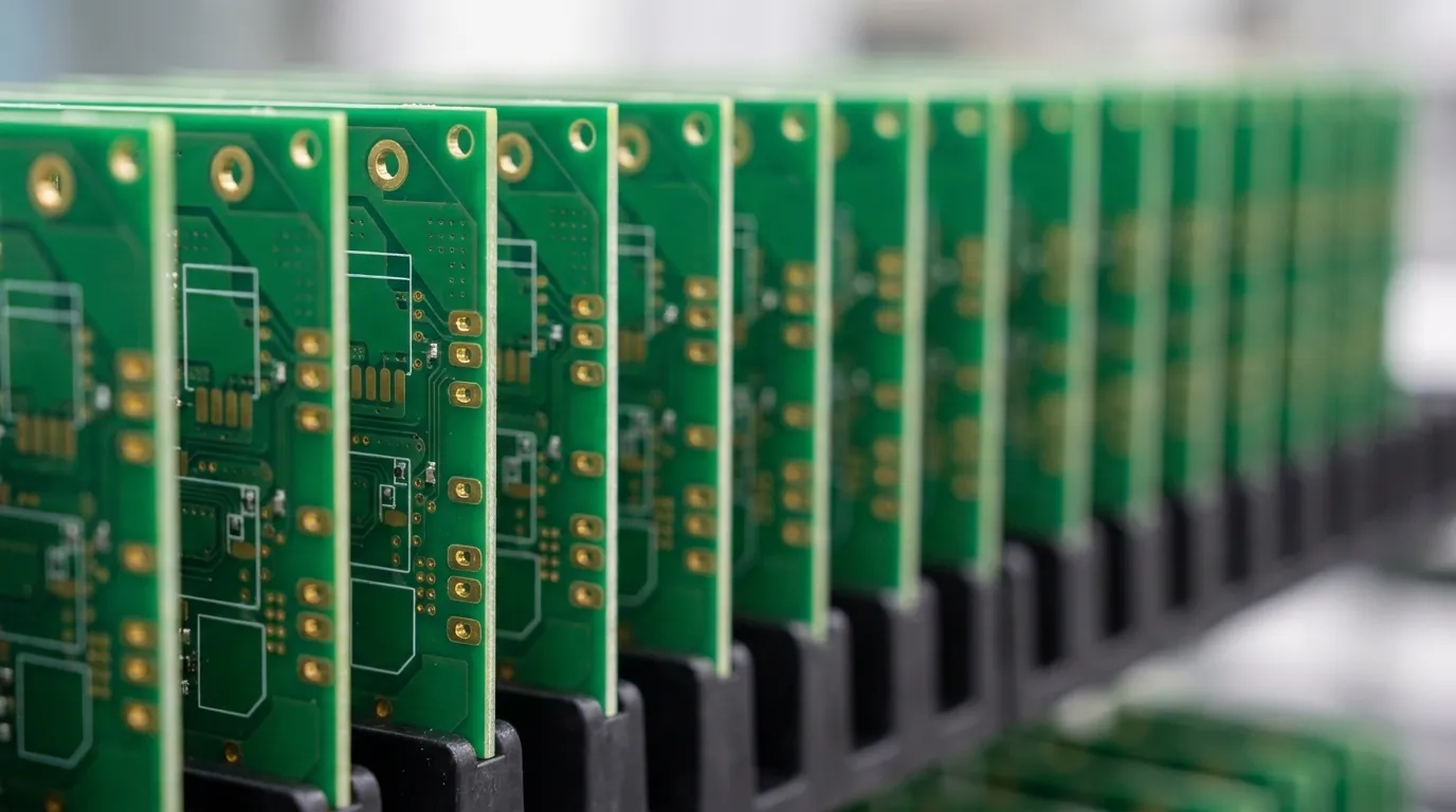
Scope of Die Attach Services for IGBT Modules
Die attach for IGBT power modules bonds a semiconductor die to a substrate or leadframe using a thermally and mechanically compliant material. The bond conducts heat away from the junction, tolerates repeated thermal expansion and contraction and maintains electrical isolation where required.
In mission-critical environments, the die attach layer often becomes a primary failure site. Next-generation IGBT modules require die attach solutions that operate at elevated junction temperatures while maintaining low thermal resistance and supporting long power-cycling life with minimal degradation. Meeting these demands requires precise material selection, tightly controlled processes and a manufacturing partner with the engineering depth to manage both.
Evaluation Framework for Die Attach Partners
Program managers and design engineers benefit from a structured checklist when assessing die attach service providers. Six connected criteria address the most common program risks and support consistent partner comparison.
Engineering integration evaluates whether the provider’s engineers join design reviews and apply design-for-manufacturability guidance before tooling. Partners with strong integration identify risks early, when design changes cost less and protect schedules.
Once DFM issues are addressed, prototyping capability determines how quickly a team validates material and process choices. A dedicated fast-turn line that uses production-equivalent processes ensures prototype data translates directly to volume builds and reduces surprises at scale.
Manufacturing scope defines the range of die attach materials and process technologies available within a single facility. A partner that supports sintering, solder preforms, conductive epoxies, vacuum reflow and bond-line inspection can align process selection with program goals instead of forcing a single default approach.
Quality and compliance posture covers certifications such as AS9100, Nadcap accreditation and ITAR registration, along with documented traceability from raw material through finished assembly. Strong quality systems connect directly to smoother audits and faster customer qualification.
Supply-chain resilience addresses counterfeit avoidance methodology, domestic sourcing options and the provider’s ability to maintain continuity when component markets tighten. Robust supply practices protect schedule commitments and reduce lifecycle risk.
Scalability confirms that the same partner who builds prototypes can support low-to-mid volume production runs without transferring the program to another facility or team. This continuity preserves process knowledge and shortens the path from engineering validation to stable production.
Material Selection Considerations for IGBT Die Attach
Three material families dominate high-reliability IGBT die attach: silver sintering, eutectic solders and conductive epoxies. Each family presents distinct trade-offs in thermal conductivity, mechanical compliance, process temperature and long-term reliability.
Silver sintering produces a porous metallic bond with thermal conductivity above conventional solders. It provides strong thermal and electrical performance together with enhanced reliability and durability, which suits wide-bandgap semiconductors in power electronics. At the elevated temperatures described earlier, sintered silver bonds extend power-cycling lifetime compared with solder alternatives. Pro-Active Engineering applies silver sintering as part of engineered thermal solutions for high-power applications.
Eutectic solders, including gold-based alloys and high-temperature lead-free formulations, remain common in aerospace and defense programs. Gold-based solders support high-reliability applications such as aerospace and military die attach where strong thermal and electrical conductivity is required. Solder preforms with controlled geometry promote consistent bond-line thickness across large-area dies. Patented InFORMS® technology further improves bond-line control and reliability and supports precision die attach applications that demand consistent bond-line thickness.
Conductive epoxies provide processing advantages at lower temperatures and accommodate coefficient-of-thermal-expansion mismatch between silicon dies and ceramic substrates. Die attach films for IGBT modules must handle this mismatch through mechanical compliance and robust adhesion to prevent delamination under thermal cycling. Epoxy-based systems suit programs where process temperature limits or substrate compatibility rule out metallic bonds, although their thermal conductivity remains lower than sintered or solder options.
Material selection for a given IGBT program depends on junction temperature targets, power-cycling requirements, substrate materials and qualification standards. Pro-Active Engineering’s engineering team evaluates these parameters during the design phase and recommends a material path that lowers overall program risk.
Process Control and Void Management Priorities
Once the material is selected, process execution becomes the primary driver of bond quality. Voids in the die attach layer increase thermal resistance and concentrate mechanical stress, which accelerates fatigue under power cycling. Void-free attachment and precise bond-line thickness control remain major technical challenges for large-area power modules, especially with die sizes above 15 mm.
Vacuum reflow and controlled-atmosphere sintering serve as key process tools for minimizing voids. Indium Corporation’s die attach solutions focus on low voiding to support strong thermal performance for high-power devices such as IGBTs. Fluxless processes remove residue that can trap voids or weaken long-term adhesion in hermetic packages.
Die attach film performance depends strongly on processing conditions such as temperature, pressure and curing time. These parameters must be controlled to achieve complete curing without voids and to maintain stable dimensions. In-process inspection and post-attach scanning acoustic microscopy or X-ray confirm that bond-line thickness and void percentage meet specification before the module advances to wire bonding or encapsulation.
Pro-Active Engineering’s in-house engineering team links process parameter development with DFM review. This integration reduces iteration cycles and lowers schedule risk on complex IGBT programs.
Request a quote to discuss process control requirements for an IGBT module program.
Reliability Testing and Qualification Protocols for IGBT Die Attach
IGBT die attach qualification draws from several overlapping standards depending on the end market. Clear alignment on applicable standards and on how a manufacturing partner supports them becomes a key differentiator in partner selection.
IEC 60747-9 defines thermal resistance measurement and testing methodologies for power semiconductor devices. It establishes critical parameters such as junction-to-case thermal resistance for evaluating die attach thermal performance in IGBT modules.
Reliability testing for IGBT die attach films often follows JEDEC JESD22-A104 and IEC 60749-5 thermal cycling protocols, along with AEC-Q101 automotive qualification that requires extended cycling without delamination. Defense and aerospace programs reference MIL-STD-883 and MIL-STD-750 for more stringent thermal and aging requirements.
AEC-Q101 serves as a primary qualification standard for discrete semiconductors, including IGBTs in automotive applications. It mandates thermal cycling across wide temperature ranges for thousands of cycles and power cycling tests that monitor electrical parameters and thermal resistance changes to assess die attach integrity.
Pro-Active Engineering operates under AS9100 certification and Nadcap accreditation, with ITAR registration supporting controlled defense and aerospace programs. Full material traceability, documented process records and first-article inspection reports support customer qualification packages and program audits.
US and Offshore Trade-offs in IGBT Packaging
Offshore IGBT packaging introduces risks that compound over a program’s lifecycle. Intellectual property exposure, counterfeit component infiltration, geopolitical supply disruptions and extended logistics cycles all increase total cost of ownership and program risk for defense and aerospace customers.
ITAR-controlled programs require manufacturing within a registered domestic facility with documented access controls. Offshore providers cannot meet this requirement without complex licensing arrangements that add administrative burden and audit exposure.
Pro-Active Engineering’s single-location facility in Sun Prairie, Wisconsin consolidates design, prototyping, die attach, advanced interconnect and system integration under one roof. All operations are ITAR-registered, Nadcap-accredited and aligned to NIST 800-171 for secure data handling. Counterfeit avoidance follows SAE AS5553B methodology, and BOM scrubbing through SiliconExpert identifies lifecycle risk before procurement.
Domestic manufacturing also supports faster design iteration. When engineering and production share a facility, DFM feedback reaches designers quickly, and prototype builds use the same equipment and processes as production runs.
Glossary of Key Die Attach Terms
Silver sintering: A die attach process that bonds a semiconductor die to a substrate by applying pressure and heat to silver particles, forming a porous metallic joint with high thermal and electrical conductivity.
Bond line thickness (BLT): The controlled thickness of the die attach material between the die and substrate after processing. Consistent BLT supports predictable thermal resistance and mechanical performance.
Void percentage: The proportion of the die attach area occupied by voids or gaps rather than bonding material. Lower void percentages correlate with lower thermal resistance and longer fatigue life.
Die shear strength: A mechanical test metric that measures the force required to shear a bonded die from its substrate. It verifies bond integrity after attach and after reliability stress testing.
Rth(j-c): Junction-to-case thermal resistance, expressed in °C/W or K·cm²/W. It quantifies how effectively heat moves from the semiconductor junction through the die attach layer to the module case.
CTE mismatch: The difference in coefficient of thermal expansion between the die and substrate materials. Large CTE mismatches generate mechanical stress during thermal cycling and can cause delamination if the die attach material lacks sufficient compliance.
Frequently Asked Questions
Recommended materials for IGBT modules above 175°C
Silver sintering is the leading material choice for IGBT modules at the elevated junction temperatures discussed earlier. Sintered silver bonds maintain structural integrity and low thermal resistance beyond the practical limits of conventional tin-based solders. Gold-based eutectic solders also appear in aerospace and military applications where process compatibility and long-term hermeticity matter. Conductive epoxies generally do not suit sustained high-temperature operation because their thermal conductivity and mechanical strength degrade more rapidly under prolonged thermal stress. Material selection should be validated against the specific junction temperature target, power-cycling profile and applicable qualification standard for the program.
Void and bond-line control in large-area IGBT die attach
Void control in large-area die attach relies on material selection, process atmosphere and inspection. Vacuum reflow and controlled-atmosphere sintering remove gas from the bond interface during processing. Solder preforms with defined geometry and sintering pastes with tuned particle size distributions reduce void nucleation sites. Tooling, applied pressure and material volume control manage bond-line thickness.
Post-attach inspection using scanning acoustic microscopy or X-ray imaging quantifies void percentage and confirms bond-line thickness before the assembly advances. Providers with in-house engineering capability can adjust process parameters quickly when inspection results fall outside specification.
Certifications and traceability standards for mission-critical IGBT packaging
Defense and aerospace IGBT programs typically require AS9100 certification as a baseline quality management standard. Nadcap accreditation covers special processes including soldering and advanced assembly operations. ITAR registration is mandatory for programs involving controlled defense articles or technical data.
Traceability requirements include documented material certifications, lot control from incoming inspection through final test and first-article inspection reports. MIL-STD-883 and MIL-STD-750 define environmental and mechanical test methods for military-grade semiconductor assemblies. AEC-Q101 applies to automotive and industrial programs. Programs with functional safety requirements may also reference ISO 26262 for failure mode analysis and reliability prediction tied to die attach thermal fatigue mechanisms.
Differences between integrated design-to-production partners and traditional EMS providers
Traditional EMS providers focus on executing a released design at volume. They receive a finalized bill of materials and assembly drawing, then build to that specification.
An integrated design-to-production partner engages earlier and applies DFM analysis during the design phase to identify thermal, mechanical and manufacturability risks before tooling. For IGBT modules, this approach establishes material selection, bond-line targets and void acceptance criteria with production process capability in mind from the start. The result is fewer late-stage engineering changes, faster qualification and a prototype-to-production transition that does not require revalidation at a different facility.
Pro-Active Engineering’s model combines engineering, advanced interconnect, thermal management and scalable assembly under one roof, giving program teams a single accountable partner across the full product lifecycle.
Conclusion: Next Steps for IGBT Programs
Die attach performance determines whether an IGBT module meets its thermal, mechanical and reliability targets. Material selection, process control, void management and qualification testing are interdependent and benefit from a partner that integrates engineering with production from the first design review.
Pro-Active Engineering applies silver sintering, direct thermal path technology, advanced interconnect and accredited quality systems within an ITAR-registered domestic manufacturing environment. This combination reduces program risk, supports full traceability and creates a seamless path from prototype to production.
Request a quote to start a conversation about die attach services for an IGBT module program.