Key Takeaways for Flip Chip EMI Shielding
-
Flip chip packaging EMI shielding applies conductive materials around the assembly to block electromagnetic interference at the package level before it reaches adjacent circuits.
-
Die-backside shielding methods such as metallic lids, conductive coatings and 5-sided metallization manage emissions from exposed silicon surfaces in high-frequency designs.
-
Coating options including silver-filled ECAs, copper metallization and hybrid absorbers must balance electrical conductivity, thermal performance and process compatibility for defense and aerospace applications.
-
Grounding strategies and thermal interface material integration prevent floating shields and maintain both EMI suppression and heat dissipation in FCBGA and SiP packages.
-
Pro-Active Engineering offers US-based, ITAR-compliant manufacturing and integrated DFM support for flip chip EMI shielding programs, with a single domestic workflow from design through production.
Die-Backside Shielding Methods for Flip Chip Packages
The exposed die backside is the primary emission surface in a flip chip package. Shielding uses a conductive layer on the silicon surface or a metallic lid that contacts the die backside through a thermally and electrically conductive interface.
Common approaches include metallic stiffener lids fabricated from copper or stainless steel alloys, which provide mechanical protection and shielding. Copper offers higher thermal and electrical conductivity, which suits high-power-density applications. Stainless steel provides rigidity and corrosion resistance where mechanical robustness is the priority.
In lidless configurations, a conductive coating is applied directly to the die backside and extended over the package sidewalls to form a continuous shield. This approach reduces package height and supports the 5-sided metallization strategies described below. In both configurations, the die-backside shield must conduct heat away from the junction and maintain electrical continuity to the ground reference on the substrate.
Conductive Coating Options and Deposition Techniques
Three coating families dominate flip chip EMI shielding: silver-filled electrically conductive adhesives, copper-based metallization and hybrid or composite coatings that combine metallic and absorbing layers.
Silver-filled ECAs achieve bulk conductivity suitable for EMI shielding applications. Silver offers higher conductivity than gold at lower cost, while gold fillers support corrosion resistance and long-term contact stability in aerospace and defense applications. Silver-filled ECAs also provide thermal conductivity alongside electrical performance, which supports heat dissipation in flip chip packages.
Copper metallization, applied by electroplating or physical vapor deposition, creates a continuous low-resistivity layer suited to 5-sided package coverage. Electroplating builds thicker layers and is cost-effective at volume. Sputtering produces conformal thin-film deposits with precise thickness control and strong adhesion, which suits fine-geometry packages and wafer-level processing.
Ultrasonic spray deposition applies conductive inks and nanoparticle suspensions with low overspray and uniform coverage over complex topographies. It is compatible with silver nanowire, carbon nanotube and hybrid formulations, and it operates at lower temperatures than sputtering, which reduces thermal stress on assembled packages.
Hybrid coatings combine a reflective metallic layer with an absorbing layer to suppress both reflected and transmitted EMI. Hybrid EMI absorber stackups include a metal shielding layer, an optional insulation layer and an absorbing layer that converts electromagnetic energy into heat. This structure provides broadband suppression in compact form factors.
The coating techniques described above are applied in different configurations depending on package geometry and shielding requirements.
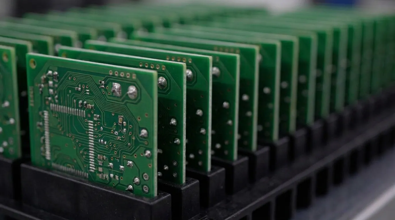
5-Sided Package Metallization for FCBGA and SiP
5-sided metallization extends a conductive layer across the top and all four lateral faces of a package, forming a near-complete Faraday cage. The bottom face connects to ground through the substrate, which completes the enclosure. This approach is standard for FCBGA and system-in-package designs where multiple die or RF components require isolation from each other and from external fields.
Silver-ink screen printing and conductive film lamination are established methods for applying the lateral and top-surface layers after singulation. Sputtering and electroless plating support tighter thickness control or finer surface conformality when required. Each method integrates into the substrate manufacturing and assembly process flow at different points, and the selection affects process yield and downstream grounding implementation.
The shield must be electrically continuous across all five surfaces and must make reliable contact with the ground ring or ground vias on the substrate edge. Without this continuity, discontinuities at package corners or at the substrate interface create gaps that allow EMI leakage and degrade shielding effectiveness. DFM review should identify and address these potential discontinuities before tape-out.
Grounding Strategies to Prevent Floating EMI Shields
A floating EMI shield, which is not referenced to a defined ground potential, can act as an antenna and worsen radiated emissions rather than suppress them. Grounding the shield to the substrate ground net is mandatory for effective shielding.
In FCBGA designs, a ground ring routed on the substrate perimeter provides the connection point for the package-level shield. Conductive-ink vias or edge-plated castellations connect the lateral metallization to that ring. The ground ring must connect to the system ground plane through multiple vias distributed around the perimeter to minimize ground impedance at high frequencies.
SiP designs with multiple shielded compartments require individual ground connections for each compartment wall. Conductive adhesive dispensed along the compartment wall base bonds the wall to the substrate ground trace and provides a low-impedance path. DFM practices for grounding include specifying minimum contact width at the shield-to-substrate interface, defining via density requirements for the ground ring and verifying continuity in the post-assembly inspection plan.
Integrating these grounding decisions into the substrate design phase, rather than resolving them at assembly, reduces rework risk and supports first-pass yield in production.
Thermal Interface Material Integration with EMI Shields
High power density in flip chip assemblies creates localized hotspots where interface thermal resistance becomes a key constraint. The EMI shield and the thermal interface material occupy the same physical space between the die backside and the heat spreader or lid, so the stack-up must satisfy both functions.
Thermal management in advanced packaging increasingly uses materials that combine adequate thermal conductivity with electrical conductivity, which allows a single layer to serve both shielding and heat-spreading roles. Silver-filled ECAs and sintered silver layers are candidates for this dual-function position. Where electrical isolation between the die backside and the lid is required, a thermally conductive but electrically insulating TIM sits between the die and a separate conductive shield layer.
The hybrid absorber stackups described earlier become particularly relevant when electrical isolation is required between the die backside and the lid. The insulation layer prevents unintended current paths while maintaining EMI suppression. Selecting the correct stack-up requires knowledge of the die backside potential, the lid or heat spreader potential and the thermal budget for the application.
CTE mismatch between silicon and organic substrates generates shear stress during temperature cycling. TIM selection must account for this stress, because rigid TIM layers can transmit mechanical load to the die or solder joints. Compliant silver-sintered or polymer-based TIMs with appropriate modulus characteristics reduce this risk in high-reliability programs.
US-Based ITAR-Compliant Manufacturing for EMI-Shielded Flip Chip
Defense and aerospace flip chip programs require full traceability, controlled processes and domestic supply chain security. Vendor fragmentation that separates substrate design, EMI shielding deposition, assembly and test across multiple suppliers introduces documentation gaps, increases program risk and complicates ITAR compliance.
Pro-Active Engineering consolidates flip chip assembly, advanced interconnect, conductive coating, thermal management and system integration under one roof in Sun Prairie, Wisconsin. The facility operates under ISO 9001:2015, AS9100, Nadcap and JCP certifications, with ITAR registration and NIST 800-171 alignment that support secure data handling for controlled programs.
DFM is embedded from the design phase. Engineering and manufacturing operate within a single workflow, so EMI shielding, grounding and thermal stack-up decisions are validated against production constraints before the design is released. This approach reduces late-stage redesigns and supports predictable transition from prototype to production volume.
Pro-Active Engineering’s CAGE Code is 7R4Q2. Programs requiring Navy and Army specification compliance, counterfeit avoidance per SAE AS5553B and IPC-A-610 Class 3 workmanship standards are supported within the same integrated workflow.
Defense and aerospace engineers working on flip chip EMI shielding programs can discuss program-specific requirements with Pro-Active Engineering’s team through a secure, US-based engagement.
Evaluating EMI Shielding Options for a Flip Chip Design
EMI shielding selection for a flip chip package rests on four interdependent criteria. These criteria are shielding effectiveness across the target frequency band, thermal performance at the die-backside interface, grounding integrity from shield to substrate ground net and compliance with domestic manufacturing and traceability requirements.
No single material or deposition method satisfies all four criteria in every case. The evaluation framework should start with the electrical and thermal budget, then define the grounding architecture at the substrate level. The coating or metallization method is then selected to fit the process flow and certification requirements of the program.
Pro-Active Engineering supports this evaluation from the design phase through production, providing an integrated US-based workflow for defense and aerospace flip chip programs. Start a technical review with Pro-Active Engineering to align shielding, thermal and manufacturing decisions.
Frequently Asked Questions
What is the best material for EMI shielding in flip chip packages?
There is no single best material. Silver-filled electrically conductive adhesives provide a balance of electrical conductivity and processability, and they are widely used for die-attach and coating applications in flip chip packages. Copper metallization applied by electroplating or sputtering delivers low resistivity and suits 5-sided package coverage. Gold-filled adhesives are preferred where long-term corrosion resistance and contact stability are the priority, as in high-reliability aerospace and defense applications. The selection depends on required shielding effectiveness, thermal budget, substrate compatibility and the certification requirements of the program.
How is an EMI shield grounded in an FCBGA without creating a floating shield?
Grounding requires a continuous low-impedance path from the shield metallization to the substrate ground net. In FCBGA designs, a ground ring routed on the substrate perimeter serves as the connection point. The lateral shield metallization contacts this ring through conductive-ink vias, edge-plated castellations or conductive adhesive applied along the package perimeter. The ground ring then connects to the system ground plane through distributed vias. The key DFM requirement is specifying minimum contact width and via density at the shield-to-substrate interface and verifying continuity in the post-assembly inspection plan. Floating shields result from discontinuities at package corners or insufficient contact area at the substrate edge, both of which are addressable in the substrate design phase.
What deposition techniques are used for 5-sided metallization?
The most common techniques are sputtering, electroless plating, electroplating, silver-ink screen printing and ultrasonic spray deposition. Sputtering produces conformal thin-film layers with precise thickness control and suits fine-geometry packages and wafer-level processing. Electroplating builds thicker layers cost-effectively at volume. Silver-ink screen printing and conductive film lamination are applied after singulation and integrate into standard package assembly flows. Ultrasonic spray deposition applies conductive inks and nanoparticle suspensions with uniform coverage over complex topographies and is compatible with lower-temperature processing. The choice depends on package geometry, required coating thickness, substrate material compatibility and production volume.
How are thermal interface materials combined with EMI shields in high-reliability applications?
The approach depends on whether the die backside and the heat spreader or lid can share an electrical potential. When they can share a potential, a single silver-filled or sintered silver layer can serve both the thermal and shielding functions, which simplifies the stack-up. When electrical isolation is required between the die backside and the lid, a thermally conductive but electrically insulating TIM is placed at the die interface, and a separate conductive shield layer is applied above it. Hybrid absorber stackups that include an insulation layer between the metallic shield and the absorbing layer address configurations where an unintended electrical path to the die backside must be avoided. In all cases, TIM compliance and modulus must accommodate CTE mismatch between the silicon die and the organic substrate during thermal cycling, which is a common reliability constraint in defense and aerospace programs.