Key Takeaways
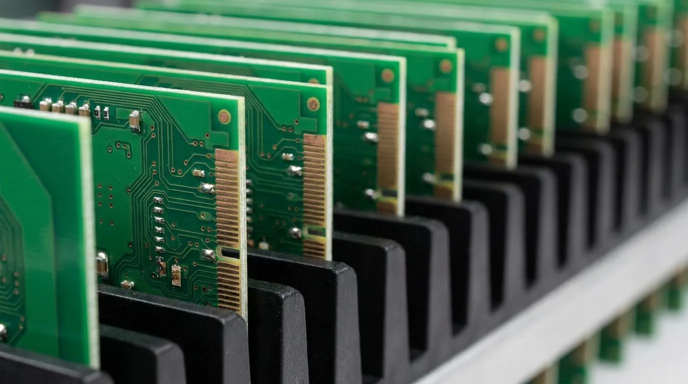
- Flip-chip technology inverts the die and uses solder or copper pillar bumps for direct electrical and mechanical connections, which increases I/O density and shortens interconnect paths compared with wire bonding.
- Substrate choice, including organic laminates, ceramic or silicon interposers, determines thermal performance, reliability and cost for high-reliability applications.
- Common package families such as FC-BGA, FCCSP, WLCSP and FCOB each balance footprint, thermal dissipation and manufacturing complexity for specific program needs.
- Advanced 2.5D/3D and chiplet integrations extend flip-chip capabilities through silicon interposers, TSVs and hybrid bonding for ultra-high-density, high-bandwidth designs.
- Pro-Active Engineering integrates packaging decisions into the design phase to support manufacturable, compliant assemblies; Request a quote to start a program.
Substrate Choices That Shape Flip-Chip Reliability
Substrate material serves as the primary variable that governs thermal performance, reliability and cost in flip-chip packages. Three substrate families cover most mission-critical applications.
Organic laminates represent the largest share of flip-chip substrate usage because they support fine-pitch routing, align with high-volume manufacturing and provide favorable electrical performance. Materials such as BT resin and ABF film are common. The limitation is a significant coefficient of thermal expansion mismatch with silicon. Silicon expands at approximately 2.6 ppm/°C while organic substrates expand at 15–18 ppm/°C, which creates thermo-mechanical stress that underfill must manage.
Ceramic substrates, including alumina and LTCC, are the preferred choice for aerospace, defense and high-power applications because their CTE is closer to silicon, they provide hermetic sealing and they maintain dimensional stability across wide temperature ranges. Higher production costs and manufacturing complexity limit their use to programs where long lifecycle and harsh-environment reliability justify the investment.
Silicon interposers enable ultra-high-density inter-chip interconnection in 2.5D and 3D advanced packages. Because the interposer shares the same CTE as the die, stress at the bump interface stays low. Silicon interposers support bandwidth and interconnect density requirements that exceed what organic substrates can handle.
Flip-Chip Package Families Used in High-Reliability Designs
FC-BGA mounts a flip-chip die on an organic or ceramic BGA substrate, combining area-array I/O with the established BGA board-attach infrastructure. This compatibility with existing assembly processes makes FC-BGA a strong choice for high I/O count processors and FPGAs in defense and aerospace systems where manufacturing maturity reduces qualification risk.
FCCSP reduces the package footprint to near die size while retaining flip-chip interconnect. It supports high pin-count applications such as 5G devices and AR glasses that demand compact form factors. The smaller substrate area limits thermal dissipation, so power budget and cooling strategy require careful evaluation.
WLCSP forms entirely at the wafer level before dicing, and the package footprint equals the die. WLCSP suits low-pin-count, space-constrained designs such as sensors and mobile controllers. It is generally limited to lower power dissipation levels because the compact size restricts thermal management options.
FCOB bonds the die directly to the PCB substrate without an intermediate package. This approach minimizes stack height and removes one substrate layer, which can reduce cost and improve signal integrity. It requires the PCB to meet the fine-pitch and surface-finish demands of direct die attach, and rework becomes significantly more complex.
Copper pillar bumps deliver lower electrical resistance, higher current-carrying capability and improved electromigration resistance. They support fine-pitch, high-reliability flip-chip assemblies in applications that combine high I/O density with demanding thermal and mechanical stress profiles.
Selecting the right combination of package family and bump technology requires matching these technical capabilities to program-specific I/O density and thermal requirements. Request a quote to discuss which configuration fits a specific program.
Advanced 2.5D, 3D and Chiplet Architectures Built on Flip-Chip
When single-die packages cannot meet bandwidth or heterogeneous integration requirements, advanced architectures build on flip-chip fundamentals by placing or stacking multiple dies within a single package. In 2.5D integration, flip-chip micro-bumps attach multiple dies side by side onto a TSV-enabled silicon interposer. The interposer routes signals between dies at densities that organic substrates cannot match. TSMC’s CoWoS places logic chips and high-bandwidth memory on a silicon interposer bonded to a package substrate.
In 3D integration, flip-chip technology combined with TSVs allows vertical chip stacking. This approach shortens interconnection lengths, increases bandwidth and reduces power consumption. Hybrid bonding advances this further by achieving Cu-to-Cu direct bonding at pitches below 1 µm, which removes bumps at the die-to-die interface.
Cu-to-Cu hybrid bonding expands as chiplet adoption accelerates and enables inter-chip spacing as low as 0.8 µm. For regulated-industry programs, these architectures introduce new qualification requirements around thermal modeling, underfill compatibility and inspection access that design teams must address early.
Fan-out wafer-level packaging extends flip-chip principles by using redistribution layers to fan out I/O ports beyond the die boundary. This method removes the need for a separate substrate and enables thinner profiles suited to space and satellite applications.
Flip-Chip and Wire Bond Compared
Wire bonding routes thin metal wires from die pads to peripheral substrate pads. The approach is mature, cost-effective and well suited to moderate I/O counts. Flip-chip distributes bumps across the full die surface, which supports I/O densities that wire bonding cannot reach at the periphery alone.
Flip-chip interconnection allows the back of the die to contact a heat sink directly. This configuration delivers lower thermal resistance than wire bonding for high-power devices. Wire-bond BGA packages conduct heat primarily through solder balls and substrate, which works for moderate power levels but becomes less efficient at high power densities.
Electrically, flip-chip shorter interconnect paths reduce parasitic inductance and capacitance. Simulations of equivalent package sizes show flip-chip configurations achieving substantially lower impedance than wire-bond counterparts at high frequencies. This difference provides a meaningful advantage for RF, mmWave and high-speed digital applications.
Wire bonding retains advantages in process maturity, rework accessibility and upfront cost. For programs where I/O counts, power density or signal integrity requirements exceed what wire bonding can deliver, flip-chip provides a more suitable path.
Flip-chip assembly requires wafer bumping, precision placement and underfill dispensing and curing. These steps add process complexity relative to wire bonding and must be executed with controlled processes and full traceability to meet aerospace and defense workmanship standards.
Manufacturing and DFM Factors for Flip-Chip Assemblies
Substrate selection drives downstream manufacturing decisions. Organic substrates require underfill to manage CTE mismatch stress. Underfill materials with high glass transition temperature, low CTE and high modulus are dispensed via capillary action after reflow and cured to disperse thermo-mechanical stress and extend solder joint fatigue life. Underfill selection must align with the operating temperature range and thermal cycling profile of the end application.
The CTE mismatch discussed earlier manifests during reflow as mechanical stress, which can cause substrate warpage, die cracking and compromised coplanarity if process parameters are not tightly controlled. Flux residue management holds equal importance, because residues can cause electrochemical migration and reduce underfill adhesion.
Inspection requirements differ by package family. FCBGA, FCCSP and WLCSP require X-ray inspection because solder joints sit under the package body. Leadframe-based flip-chip variants with wettable flank designs support automated optical inspection of solder fillets, which simplifies board-level quality verification.
For ITAR-registered programs, manufacturing must occur within a controlled domestic environment with documented chain of custody. Traceability requirements in aerospace and defense programs extend to substrate lot, bump material, underfill batch and assembly process records. IPC-A-610 Class 3 workmanship standards apply to most mission-critical flip-chip assemblies and J-STD-001 governs soldering processes throughout.
DFM review at the package selection stage prevents late-stage redesigns. Pad geometry, solder mask defined versus non-solder mask defined land patterns, via-in-pad design and PCB surface finish all affect bump collapse behavior and joint reliability. Integrating these checks before layout completion removes common sources of assembly yield loss.
Pro-Active Engineering integrated workflow embeds DFM into the design phase. Request a quote to engage engineering support before layout begins.
Using Application Requirements to Drive Package Selection
I/O count serves as the first filter. Designs with moderate I/O counts and cost sensitivity may be well served by wire-bond BGA or FCCSP. Designs that exceed the practical limits of peripheral routing require FC-BGA or advanced 2.5D integration.
Power density determines substrate and thermal interface requirements. High-power applications in defense radar, power conversion and medical imaging benefit from ceramic substrates or direct thermal path designs that reduce junction-to-board thermal resistance. Lower-power, space-constrained designs can use WLCSP or FCCSP on organic substrates with appropriate underfill.
Environmental stress profiles shape material and process choices for long-service programs. Temperature cycling range, vibration spectrum and humidity exposure all affect underfill selection, bump material choice and substrate type. Automotive-grade flip-chip lines using copper pillar joints and high-temperature underfills are qualified to AEC-Q100 Grade 0 for temperatures above 200°C. This example shows how qualification standards map to specific material and process selections.
Production volume influences the economics of advanced packaging. High-volume programs can absorb the qualification cost of copper pillar bumping and advanced substrates. Lower-volume, high-mix defense and medical programs benefit from a manufacturing partner with flexible processes and engineering depth that support complex builds without strict minimum volume constraints.
Early collaboration with a single accountable partner reduces the risk of misalignment between package selection, PCB design and assembly process. Pro-Active Engineering supports programs from initial package trade studies through advanced interconnect assembly, conformal coating and system integration under one roof with ITAR registration, AS9100 and Nadcap accreditation covering the full workflow.
Frequently Asked Questions
What are the different types of chip packaging?
IC packages are broadly classified by interconnect method and form factor. Wire-bond packages route metal wires from die pads to substrate pads and include DIP, QFP, BGA and WB-BGA families. Flip-chip packages invert the die and connect through solder or copper pillar bumps, including FC-BGA, FCCSP, WLCSP and FCOB. Advanced packages such as 2.5D silicon interposer assemblies and 3D stacked die with TSVs extend flip-chip principles to multi-die heterogeneous integration. Each family involves trade-offs in I/O density, thermal performance, process complexity and cost that must align with application requirements.
What are the three levels of chip packaging?
Chip packaging is organized into three hierarchical levels. First-level packaging encloses the bare die in a protective structure and creates the electrical interface, covering all IC package types from wire-bond to flip-chip. Second-level packaging refers to the attachment of the packaged IC to a printed circuit board using solder joints, press-fit contacts or other board-attach methods. Third-level packaging encompasses the integration of populated PCBs into a larger system or enclosure, including box build and system integration. Reliability requirements and inspection standards apply at each level, and decisions made at the first level directly affect assembly yield and long-term performance at the second and third levels.
Flip-chip vs wire bond: which offers better thermal performance?
Flip-chip generally delivers better thermal performance for high-power devices. The inverted die orientation allows the die back to contact a heat spreader or thermal interface material directly, which creates a low-resistance path from junction to heat sink. Bumps also conduct heat from the active face to the substrate. Wire-bond packages route heat primarily through the die attach material and substrate, which introduces additional thermal resistance. For applications with moderate power dissipation, wire bonding may be sufficient. For high-power-density designs in radar, power conversion or high-performance computing, flip-chip thermal path advantages often drive package selection.
What manufacturing standards apply to high-reliability flip-chip assemblies?
High-reliability flip-chip assemblies for aerospace, defense and medical applications follow several overlapping standards. IPC-A-610 Class 3 defines workmanship acceptability criteria for mission-critical electronics. J-STD-001 covers soldering materials and processes. IPC-7711/7722 addresses rework and repair. AS9100 provides the quality management framework for aerospace programs. ITAR registration is required for assemblies involving defense-related technical data or hardware. Nadcap accreditation covers special processes such as soldering and conformal coating for aerospace and defense customers. Full traceability documentation, including substrate lot records, bump material certifications and process traveler data, is expected for programs with long service life requirements.
Conclusion: Partner Early for Reliable Flip-Chip Integration
Flip-chip package selection directly affects I/O density, thermal performance and long-term reliability in mission-critical systems. The choice of substrate family, bump material, underfill and inspection method must align with the power profile, environmental stress and compliance requirements of the end application. Decisions made late in a program, after layout completion or tooling release, become the most costly to correct.
Pro-Active Engineering provides advanced interconnect and packaging capabilities, including flip-chip assembly and hybrid high-density assemblies, within an integrated design-to-production workflow. ITAR registration, AS9100 certification and Nadcap accreditation support a wide range of regulated-industry requirements. DFM enters at the design phase, not after the fact.
Programs that engage engineering support at the package selection stage reduce redesign risk, shorten qualification cycles and reach production with assemblies that perform as intended. Request a quote and connect with the Pro-Active Engineering team to begin the conversation.