Key Takeaways
-
Chiplets flip chip packaging delivers high-density integration with micro-bumps that support strong electrical and thermal performance in AI, HPC and aerospace systems.
-
Core processes include die bumping, thermal compression bonding, underfill encapsulation and advanced testing that support reliable 2.5D and 3D stacks.
-
Compared with wire bonding, flip chip supports higher I/O density, lower inductance, better power efficiency and improved yields from modular designs.
-
Design for manufacturability strategies address thermal mismatch, warpage and alignment through early simulations and CTE-matched materials.
-
Pro-Active Engineering provides ITAR-compliant flip chip assembly that reduces prototype risk and accelerates time to market.
Chiplets and Flip Chip Packaging for High-Density Systems
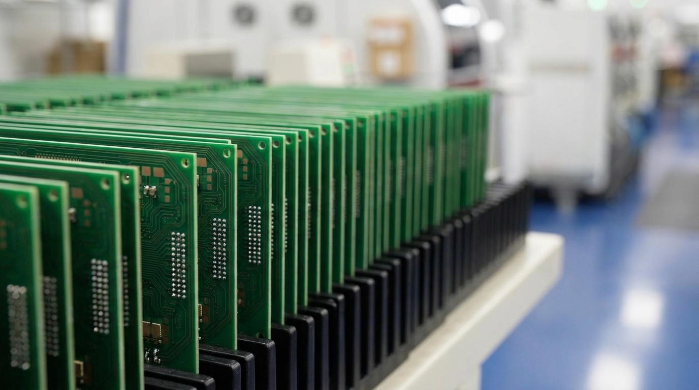
Chiplets are specialized integrated circuits designed for specific functions. They provide strong yield cost efficiency and design flexibility compared with monolithic dies. Flip chip packaging flips dies and bonds them with micro-bumps, typically solder or copper pillars, to create short chiplet interconnects that support high-speed signaling and dense integration.
Flip chip packaging provides several connected advantages over wire bonding for chiplet applications. The primary advantage is interconnect density, since micro-bumps support many more I/O connections in the same footprint than wire bonding. This density enables both vertical and lateral integration strategies. Through-silicon vias, or TSVs, support vertical routing in 3D stacks, while silicon or glass interposers support 2.5D heterogeneous integration across a single plane. Underfill materials then protect these dense interconnects during thermal cycling and mechanical stress.
Rapidus outlines the standard flip chip bump bonding sequence for chiplets as bump formation via electroplating, dicing with micrometer-level accuracy, flip chip bonding using heat and pressure, underfill application, resin molding and comprehensive testing. This sequence supports modular, high-performance architectures that power next-generation computing systems. Understanding how this sequence operates provides context for the detailed manufacturing steps that follow.
Step-by-Step Chiplets Flip Chip Packaging Process
The chiplets flip chip packaging manufacturing process follows a precise sequence designed for high-yield production.
-
Die preparation and bumping: Copper pillar electroplating creates micro-bumps on intact wafers with tight pitch control.
-
Flux application and alignment: Advanced placement systems apply flux and position each die with high accuracy.
-
Reflow or thermal compression bonding: Controlled heat and pressure create strong metallurgical bonds between bumps and pads.
-
Underfill encapsulation: Polymer materials fill gaps between die and substrate to increase mechanical stability and reliability.
-
Lid attachment and thermal management: Heat spreaders or thermal interface materials improve heat dissipation from high-power regions.
-
Testing and singulation: Electrical verification and mechanical separation complete the assembly and prepare units for downstream processes.
Each step requires tight process control to maintain yield and reliability. Manufacturing automation addresses critical challenges such as warpage control and alignment precision. Advanced flip chip bonders emphasize higher accuracy and throughput to support finer bump pitches and interconnects required for chiplet-based designs. Pro-Active Engineering applies this automation across an end-to-end PCBA workflow that maintains smooth transitions from prototype through production.
Discuss automation-focused chiplets flip chip packaging needs with Pro-Active Engineering’s team to align process capabilities with project goals.
Bonding Techniques That Enable Advanced Chiplet Designs
Specific bonding techniques support different performance, cost and density targets in chiplets flip chip packaging.
-
Solder micro-bumps: Reflow processes support standard pitch applications with strong cost efficiency.
-
Thermal compression bonding: This method suits fine pitch applications that require tight warpage control and low defect rates.
-
Copper-to-copper hybrid bonding: Direct copper interfaces provide ultra-low resistance connections for demanding performance targets.
2.5D packaging uses interposers with TSVs for lateral chiplet communication across a shared substrate. 3D stacking supports vertical integration through direct die-to-die connections. TSV arrays with micro-bumps at fine pitch achieve higher bandwidth density than wire bonding or flip chip on organic substrates, which supports the data throughput needs of AI and HPC workloads.
Performance Benefits Over Traditional Packaging
Chiplets flip chip packaging delivers measurable advantages compared with traditional packaging approaches.
-
Higher density and bandwidth: Flip chip technology enables thousands of connections between microchips and substrates using small solder balls. This density supports the bandwidth levels required for AI and HPC applications.
-
Superior power efficiency: Shorter, lower inductance paths reduce power consumption and support higher operating frequencies.
-
Enhanced yields and scalability: Breaking large monolithic dies into smaller chiplets avoids the yield cliff of large dies that exceed reticle limits, since smaller dies provide higher per-die yields and show less sensitivity to process defects.
-
Design modularity: Heterogeneous integration reduces monolithic design risk and supports targeted performance tuning for each function.
For aerospace and defense programs, flip chip packaging supports the reliability and performance density required for mission-critical systems. Short electrical paths in flip chip designs, compared with wire bonding, support faster signal propagation and reduced electromagnetic interference. These traits align with the needs of high-performance computing, radar and advanced sensing platforms.
Manufacturing Challenges and DFM Strategies
Successful chiplets flip chip packaging depends on addressing several manufacturing challenges through coordinated design for manufacturability strategies. Thermal mismatch between dies, substrates and interposers can drive warpage, which then affects alignment during bonding. CTE-matched materials reduce this mismatch at the source, while thermal simulations predict warpage behavior and guide total thickness variation targets.
Yield risk also depends on early DFM integration. High-aspect-ratio TSVs and precise TSV reveal processes create yield and cost challenges, especially as pitches scale for next-generation HBM and chiplet-based AI accelerators. Pro-Active Engineering addresses these issues through integrated engineering workflows, tuned thermal paths and DFM practices that start at the first design stages.
The thermal modeling, materials selection and process tuning described earlier must occur during initial design phases, not as late corrections. Pro-Active Engineering’s approach embeds these DFM considerations from day one to reduce risk before projects reach production volumes.
Selecting a Chiplets Flip Chip Manufacturing Partner
Choosing a manufacturing partner for chiplets flip chip packaging requires clear evaluation criteria. US-based operations with ITAR compliance support defense and aerospace programs. ISO 9001:2015 and AS9100 certifications confirm mature quality management systems. Proven flip chip and hybrid assembly experience, combined with advanced interconnect capabilities, supports complex designs. Scalable capacity from prototype through production maintains continuity as volumes grow.
Pro-Active Engineering stands out through combined flip chip and wire bonding capabilities, domestic supply chain traceability and integrated workflows that remove vendor fragmentation. A single-facility model reduces communication gaps and supply chain exposure compared with offshore or multi-vendor approaches.
Pro-Active Engineering’s ITAR-compliant operations, Nadcap accreditation and certified quality systems support secure, traceable manufacturing for regulated sectors. An integrated engineering and manufacturing workflow reduces prototype-to-production disconnect and maintains clear visibility across each project stage.
Request a quote to review Pro-Active Engineering’s chiplets flip chip packaging capabilities for specific application requirements.
Applications and Emerging Trends in Chiplets Flip Chip
Chiplets flip chip packaging supports breakthrough performance across several application domains. AI accelerators use 2.5D integration to combine GPU dies with high-bandwidth memory stacks, which supports the data throughput required for machine learning workloads. Satellite platforms apply compact, high-density integration in space-constrained designs where reliability and performance density carry high priority.
The AI chip market now drives significant package substrate demand. Growth comes from AI and high-performance computing applications that require ultra-low loss substrates. This trend reflects broad adoption of chiplets flip chip packaging in modern computing systems.
Future developments include finer pitch interconnects, integrated thermal management solutions and broader use of glass interposers for improved electrical behavior. These advances will expand the capabilities of chiplets flip chip packaging for demanding workloads.
Conclusion: Partnering for Advanced Chiplet Packaging
Chiplets flip chip packaging forms a core technology for next-generation AI, HPC and aerospace systems that require dense, high-performance integration. Clear knowledge of processes, benefits and manufacturing challenges supports strong project planning and execution. Pro-Active Engineering’s capabilities, from design through production, provide the expertise and reliability that mission-critical applications demand.
Contact Pro-Active Engineering for a design review to de-risk a chiplets flip chip packaging project and apply proven experience in advanced interconnect solutions.
Frequently Asked Questions
What is the difference between flip chip and wire bonding for chiplets?
Flip chip packaging provides shorter electrical paths and higher connection density compared with wire bonding. Wire bonding uses thin wires to connect die pads to package leads. Flip chip uses micro-bumps directly on the die surface. This structure reduces inductance, limits parasitic effects and supports higher bandwidth that aligns with chiplet requirements.
How does 2.5D packaging work with chiplets?
2.5D packaging places multiple chiplets side by side on a silicon or glass interposer that contains TSVs and redistribution layers. The interposer acts as a high-density interconnect highway that supports higher bandwidth and lower latency than traditional package-level connections. This structure also supports heterogeneous integration of dies from different process nodes and foundries.
What industries benefit most from chiplets flip chip packaging?
Aerospace, defense and high-performance computing sectors gain strong advantages from chiplets flip chip packaging. These applications require high reliability, compact form factors, strong electrical performance and integration of specialized functions. The modular nature of chiplets also supports cost control by matching process nodes to specific functions inside a single package.
Why choose a US-based manufacturer for chiplets flip chip packaging?
US-based manufacturing supports ITAR compliance for defense programs, reduces supply chain risk, improves communication and shortens logistics cycles. Domestic production also supports stronger intellectual property protection and avoids geopolitical exposure linked to offshore manufacturing. For mission-critical work, secure and traceable US-based operations provide clear advantages.
How can engineers ensure DFM success in flip chip designs?
DFM success depends on early collaboration between design and manufacturing teams, thermal modeling that addresses CTE mismatches, careful warpage control and appropriate material and process selection. Integrated engineering workflows that include manufacturing constraints from initial design phases prevent costly redesigns and support smooth transitions from prototype to production.
What are thermal compression bonding chiplets?
Thermal compression bonding, described earlier in the bonding techniques section, differs from traditional reflow because it applies force during bonding. This force supports finer pitch connections and reduces void formation. The method becomes the preferred choice when bump pitch falls below specific thresholds or when applications cannot tolerate the thermal exposure of full reflow.