Key Takeaways
-
ICT detects critical defects such as solder bridges, open circuits, tombstoning and via cracks that threaten high-reliability PCBAs in aerospace and defense.
-
Demanding environments amplify defects through vibration, thermal cycling and contamination, so programs require robust prevention strategies.
-
Common defect causes include reflow inconsistencies, solder paste variation, component selection errors and fixture problems during testing.
-
Integrated testing that combines ICT, AOI, flying probe and functional tests increases defect detection and reduces false positives.
-
Pro-Active Engineering’s end-to-end DFM, testing and ITAR-compliant manufacturing prevents ICT defects and strengthens PCBA reliability by design.
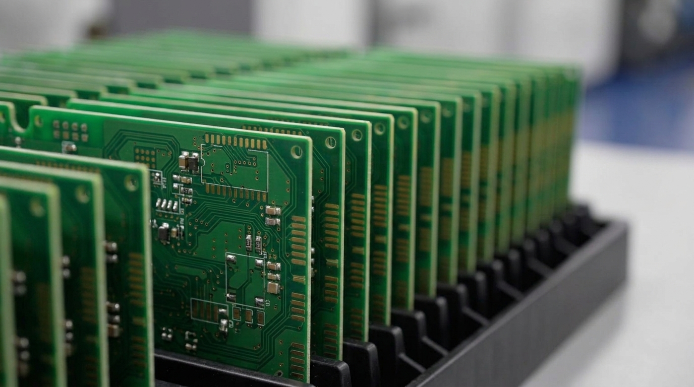
ICT’s Role in High-Reliability PCBA Performance
In-circuit testing uses bed-of-nails or flying probe systems to detect assembly defects early in the manufacturing process. For high-reliability applications, ICT typically combines with automated optical inspection (AOI) and burn-in testing to meet IPC-A-610 Class 3 and J-STD-001 requirements. Failures in high-reliability assemblies often stem from upstream soldering, cleaning or handling issues, such as inconsistent reflow profiles and paste deposition, which create weakened joints that fail under vibration or thermal cycling.
These conditions increase defect risk compared with commercial applications. PCBAs may pass initial tests but degrade over time due to material fatigue or mechanical stress from thermal cycling, humidity, vibration and chemical exposure. Detecting these latent issues requires comprehensive testing at multiple stages. Pro-Active Engineering’s approach combines flying probe, in-circuit testing, functional testing and AOI to catch defects before assemblies reach critical missions.
Common ICT Defects in High-Reliability PCBAs
ICT detects multiple defect categories that threaten high-reliability PCBA performance. The most prevalent issues include solder bridges and shorts, open circuits and missing components, tombstoning, component value errors and polarity reversals, reflow failures, IC pin problems, via cracks, ESD damage and thermal cracking that leads to vibration-induced opens.
Solder Bridges and Shorts in Dense Designs
Solder bridges create unintended electrical connections between adjacent pins or traces. In high-density assemblies, fine traces and tight spacing cause impedance mismatches that trigger signal reflections, data errors or system failures in high-speed and high-frequency applications. ICT identifies these shorts through resistance measurements between carefully placed test points.
Open Circuits and Missing Components
Open circuits represent one of the most common PCB failures. They often result from physical damage such as lifted pads with process-driven root causes. Missing components create obvious opens that ICT identifies through continuity checks and component presence tests.
Tombstoning in Thermal Cycling Environments
Tombstoning occurs when one end of a component lifts during reflow and creates an open circuit. This defect arises from reflow conditions and paste imbalance. It often affects fine-pitch components in aerospace assemblies where thermal cycling increases mechanical stress on solder joints.
Component Value Errors and Polarity Issues
Incorrect component values or reversed polarity can pass visual inspection but cause circuit malfunction. ICT detects these problems through component value measurements and polarity checks. This capability is critical in mission-critical applications where component accuracy directly affects performance and safety.
Reflow Failures from Paste and Profile Issues
Insufficient solder paste deposition in aerospace SMT printing can create weak solder joints or unstable wetting behavior, while excess deposition increases risks of bridging, poor stand-off control and rework. These risks increase because high-reliability assemblies operate within narrower process windows and face harsher environments.
Via Cracks, ESD Damage and Hidden Defects
Microvias in HDI PCBs are prone to internal defects that remain difficult to detect even with X-ray inspection. Risks increase in assemblies that experience repeated thermal cycling and pack components at high density. In high-density or miniaturized layouts, X-ray inspection identifies voids, insufficient solder and misaligned pads beneath components such as BGAs, which complements ICT coverage.
Environmental and Test Challenges in Harsh Conditions
High-reliability PCBAs face unique challenges that amplify common defects. Intermittent faults such as thermal drift or signal instability emerge under specific operating conditions or extended use and can degrade mission performance. Among these challenges, vibration-induced failures represent a particular concern because they affect both the assembly and the testing process. Pneumatic pressure on thin boards can cause ICT fixture warp and probe skips, issues that worsen under the vibration conditions these assemblies must withstand.
Environmental contamination also affects testing reliability. IPC-5704 defines cleanliness requirements for unpopulated printed boards. Residues increase resistance and cause false opens during ICT. Problems intensify when assemblies experience thermal cycling. Latent printing defects such as hidden variation in solder paste transfer can pass early inspections. These hidden issues often appear later as reliability failures under prolonged vibration, thermal cycling and mission-critical operation.
A case study illustrates how design data and fixture issues interact with these conditions. Gerber drill omissions and CAD probe coordinate drifts caused via skips, node coverage gaps and false opens in ICT testing. Pro-Active Engineering’s design-for-manufacturability approach addresses these issues early in the development process and prevents costly defects in production. Learn how integrated DFM and testing can address specific environmental and test challenges for complex programs.
Defect Prevention and Process Best Practices
Effective ICT defect prevention starts with design-for-manufacturability integration at project inception. Early DFM analysis identifies potential assembly issues before they reach production and establishes the foundation for quality. Building on this foundation, process controls such as SiliconExpert component verification help avoid counterfeit parts and obsolescence risks. These technical controls operate within a quality framework defined by adherence to ISO 9001, AS9100 and Nadcap standards.
Pro-Active Engineering’s end-to-end approach eliminates vendor fragmentation by consolidating design, rapid prototyping, assembly, testing and system integration under one roof. This integrated workflow enables smooth transitions from concept to production while maintaining full traceability and documentation required for high-reliability applications. The company’s ITAR registration and compliance capabilities support secure domestic manufacturing for defense and aerospace programs.
Comparing ICT, Flying Probe and Functional Testing
Different testing methods provide complementary coverage for high-reliability PCBAs. Flying probe testing offers flexibility and low fixture cost for prototype and low-volume builds. Traditional bed-of-nails ICT delivers faster throughput and deeper coverage for higher volumes. ICT reduces field returns according to JEDEC JESD22 reliability data. This multi-method approach, described earlier, maximizes defect detection while minimizing false positives. The combined strategy provides strong coverage for mission-critical applications and supports consistent reliability across program lifecycles.
Frequently Asked Questions
Most Common ICT Defects in High-Reliability PCBAs
The most common ICT defects include solder bridges and shorts, open circuits from missing components or lifted pads, tombstoning in fine-pitch components, component value errors and polarity reversals, reflow failures from inconsistent solder paste deposition, via cracks in high-density interconnects and thermal cracking that leads to vibration-induced opens. These defects create particular risk in aerospace, defense and medical applications where environmental stresses such as thermal cycling and vibration amplify failure rates.
How ICT Detects Open Circuits in Dense Assemblies
ICT detects open circuits by measuring resistance between test points using flying probe or bed-of-nails fixtures. The system applies test signals and measures responses to identify breaks in electrical continuity. In high-density assemblies, precise probe alignment and robust fixture design reduce false opens. Advanced ICT systems distinguish between true opens and contact issues through multiple measurement techniques and statistical analysis of test results.
Key Practices to Prevent Tombstoning
Tombstoning prevention requires careful control of solder paste printing, component placement and reflow profiling. Effective strategies include refining stencil design for consistent paste deposition, maintaining proper component placement pressure and alignment, controlling reflow temperature ramps for even heating and designing pad geometries that promote balanced wetting forces. Design-for-manufacturability analysis during layout identifies components at risk for tombstoning and supports targeted preventive measures.
ICT Support for Aerospace and Defense Compliance
ICT supports compliance by providing documented test results and traceability required by AS9100 and ITAR regulations. The testing process generates detailed reports that show component values, electrical continuity and performance parameters. Combined with controlled documentation and mature quality management systems, ICT helps demonstrate compliance with military and aerospace standards. Test data becomes part of the permanent record for each assembly and supports long-term reliability tracking and failure analysis.
Benefits of Integrated Testing Workflows
Integrated testing workflows combine ICT with inspection methods such as AOI, X-ray and functional testing under unified process control. This approach provides broad defect coverage and reduces handling between test stations. Benefits include improved correlation between test methods, faster throughput, lower risk of handling damage and consolidated documentation. For high-reliability applications, integrated workflows support stronger root cause analysis and process improvement while maintaining the traceability and quality control required for mission-critical systems.
Secure Reliability with Pro-Active Engineering
Common ICT defects in high-reliability PCBAs create significant risk for mission-critical applications, yet structured detection and prevention strategies can control these threats. Pro-Active Engineering’s integrated design-to-production workflow combines comprehensive DFM analysis, advanced testing capabilities and ITAR-compliant manufacturing to deliver assemblies that meet demanding aerospace, defense and medical requirements. This consolidated workflow, mentioned earlier, supports full compliance with quality and security standards while preserving the efficiency advantages of single-source manufacturing. Connect with Pro-Active Engineering’s team to discuss how proven testing and manufacturing expertise can enhance the reliability of high-performance PCBAs.