Key Takeaways for In-Circuit Testing on PCBs
- In-circuit testing (ICT) verifies PCB electrical integrity by measuring components and connections with bed-of-nails fixtures or flying probes, detecting opens, shorts and wrong values.
- The 7-step ICT process covers fixture setup, netlist import, probing, guarding, component checks, defect flagging and traceability reporting for thorough assembly review.
- Bed-of-nails testing fits high-volume production for speed, while flying probe supports prototypes and low-volume runs without custom fixtures.
- ICT detects assembly defects that visual inspection misses, but it cannot verify unpowered IC functionality, so teams pair it with AOI, functional and boundary scan testing.
- Pro-Active Engineering integrates ICT into certified workflows from prototypes through production; request a quote to ensure defect-free PCBA with compliance.
ICT Basics and Onshoring Context for Hardware Teams
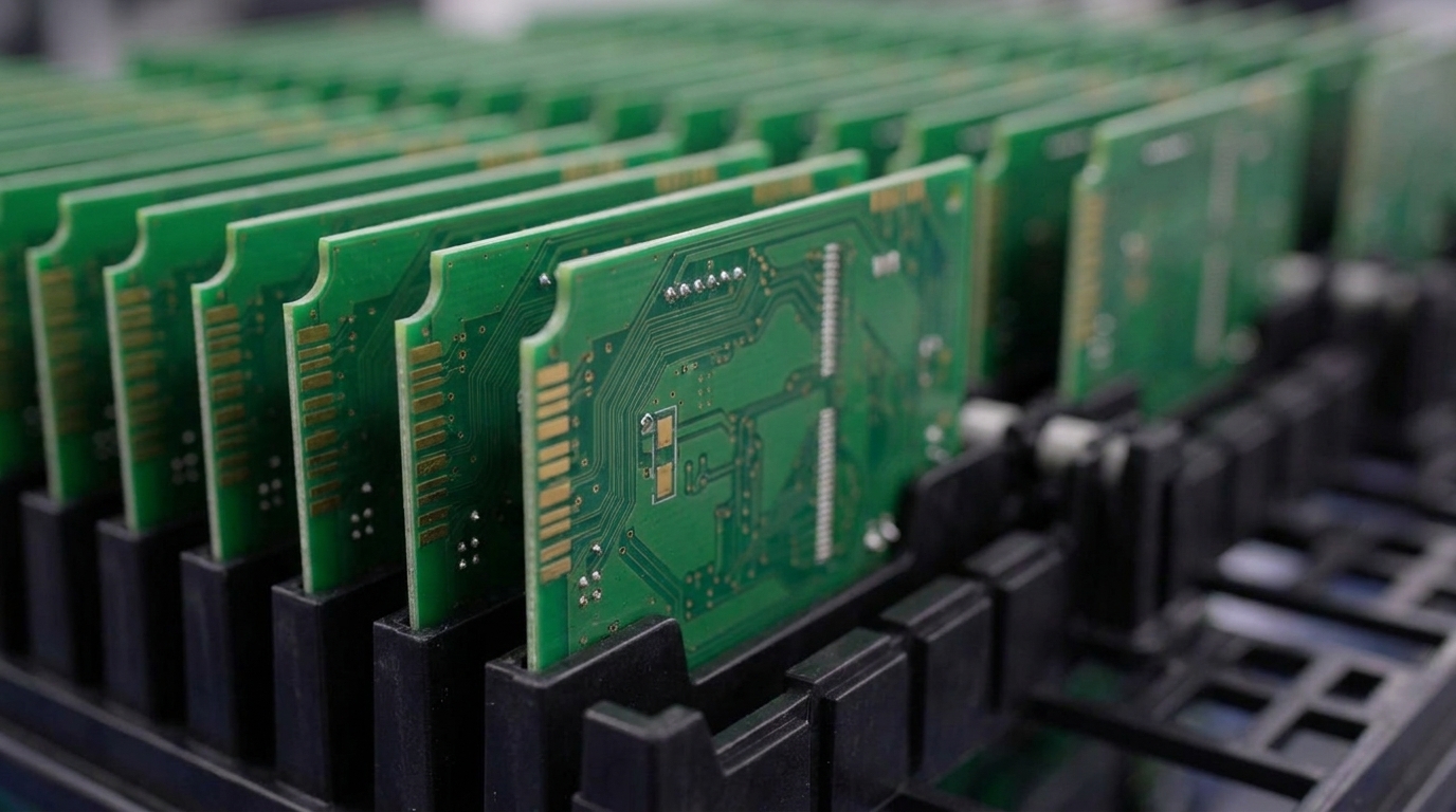
In-circuit testing operates as an unpowered electrical verification method that measures individual components and connections on assembled PCBs. Key terminology includes bed-of-nails fixtures with arrays of spring-loaded pins, pogo pins as individual test probes, guarding for isolation, netlists as electrical connection maps, flying probe systems with movable test heads and AOI for automated optical inspection.
The current trend toward US onshoring increases demand for domestic PCBA partners that deliver rapid prototyping and production-scale testing in one location. Pro-Active Engineering addresses this need through a single-location workflow that integrates design, Speed Shop prototyping and comprehensive testing under one roof. Request a quote to explore how this integrated approach streamlines development timelines.
Core Components That Make In-Circuit Testing Work
Bed-of-nails fixtures form the foundation of production ICT systems. These fixtures feature spring-loaded pins that maintain reliable electrical contact while accommodating minor board warpage.
Test programs control the measurement sequence using netlists extracted from PCB design files and bill of materials data. These netlists define which connections the system verifies, and guarding circuits then isolate each target net from parallel paths that could distort readings. This isolation supports an unpowered testing approach that protects sensitive components while still confirming assembly integrity.
Pro-Active Engineering designs high-density fixtures that reach fine-pitch test points on complex assemblies. The fixture development process applies DFM principles to balance strong test coverage with efficient manufacturing.
Step-by-Step ICT Process on PCBs: 7 Practical Stages
1. Fixture setup and board loading: The operator places the PCBA into the fixture nest where registration pins match the PCB tooling holes and align the board so probes land accurately on target test points. Vacuum or pneumatic systems secure the board for consistent contact.
2. Netlist and BOM import: Test software imports electrical connection data from design files and the BOM. It then generates measurement sequences that check each component and connection against defined specifications.
3. Probing and signal application: Spring-loaded pins make simultaneous contact with designated test points. They apply low-level DC and AC signals that measure resistance, capacitance and inductance values across the circuit.
4. Guarding isolation: Advanced guarding techniques isolate individual nets from parallel circuit paths. These techniques maintain accurate measurements even on complex high-density designs.
5. Component verification: The system measures component values and verifies diode polarity. It flags any deviation from design specifications.
6. Defect flagging and reporting: Test software compares measurements against programmed limits. It immediately identifies opens, shorts, wrong component values and assembly defects, then records diagnostic information.
7. Data output and traceability: Results generate detailed reports for quality documentation. These reports support full traceability requirements in regulated industries.
Pro-Active Engineering integrates ICT with AOI and functional testing for comprehensive defect detection. Request a quote for ICT implementation that scales from prototypes to production volumes.
Comparing Bed-of-Nails and Flying Probe ICT Methods
Bed-of-nails fixtures contact all test points simultaneously, enabling high throughput that fits production volumes. Fixture-based testing scales efficiently for medium- to high-volume production but requires investment in custom tooling.
Flying probe testing uses sequential probing. It fits prototypes and low-volume production, and flying probe testing requires no fixtures, which shortens early development setup.
For testing ICs on PCBs, guarding becomes critical to isolate complex integrated circuits from surrounding components. This isolation challenge grows with fine-pitch packaging, where flying probe systems excel because movable probes reach tight spaces that bed-of-nails fixtures cannot access.
Pro-Active Engineering employs both methods in a coordinated strategy. The team uses flying probe testing for Speed Shop prototypes and design validation, then transitions to bed-of-nails fixtures for production volumes where throughput and repeatability matter most.
ICT Defects Found on PCBs and Method Limits
In-circuit testing excels at detecting assembly-related defects including opens, shorts, wrong component values, polarity errors, missing components and solder joint integrity issues. Solder bridging caused by excessive solder paste volume represents a common defect that ICT identifies through resistance measurements between adjacent nets.
ICT limitations stem from its unpowered nature and physical access constraints. The unpowered approach prevents verification of integrated circuit functionality, while high-density layouts reduce accessible test points and parallel circuit paths can still interfere with measurements. These factors explain why comprehensive strategies combine ICT with boundary scan for complex ICs and functional testing for powered verification.
Pro-Active Engineering addresses ICT limitations through a multi-layered approach that includes 100% AOI for mechanical defects, comprehensive ICT for electrical checks and functional testing for system-level validation.
How ICT Fits Within Seven PCB Testing Methods
The seven primary PCB testing methods each address specific verification needs. Visual inspection catches obvious assembly errors, AOI detects component placement and solder joint issues, ICT verifies electrical integrity, flying probe supports flexible low-volume testing, functional testing validates powered operation, X-ray inspection reveals hidden solder defects and burn-in testing stresses components under extended operation.
ICT occupies the electrical verification stage between mechanical assembly inspection and functional system testing. This position allows ICT to catch defects that visual methods miss while still providing faster feedback than full functional testing.
Pro-Active Engineering implements this complete testing suite, which delivers broad defect coverage across mechanical, electrical and functional domains for mission-critical applications.
Integrating ICT into a Prototype-to-Production Workflow
Effective ICT integration starts during the design phase with DFM decisions that preserve test point access and spacing. The integrated workflow mentioned earlier incorporates testability analysis during PCB layout and prevents costly redesigns when projects move from prototypes to production.
Speed Shop prototyping uses flying probe testing to confirm electrical integrity on initial builds and gathers data that guides bed-of-nails fixture design for production scaling. Recent advances in AI-driven test optimization strengthen this transition by supporting more sophisticated guarding strategies and improved defect detection algorithms.
Nadcap-accredited processes then keep ICT implementation aligned with aerospace and defense quality requirements from prototype through production, maintaining consistent performance across the entire product lifecycle.
Common ICT Challenges and Practical Fixes
Probe misalignment represents the most frequent ICT challenge and often results from PCB warpage, fixture wear or weak registration. Reliable bed-of-nails fixtures maintain precise probe positioning through robust mechanical construction and appropriate contact force, which reduces these issues.
Guarding errors create false failures when parallel circuit paths interfere with measurements. Strong test program development includes detailed guarding analysis that isolates target components from surrounding circuitry and reduces nuisance faults.
High-density designs strain traditional ICT approaches because of limited test point access and fine-pitch spacing. Pro-Active Engineering addresses these designs with advanced fixture techniques and hybrid strategies that combine ICT with complementary methods.
Measuring ICT Success and Partnering with Pro-Active Engineering
ICT effectiveness metrics include first-pass yield improvement, defect detection rates and false positive reduction. Properly implemented bed-of-nails ICT achieves high test coverage when PCBs follow sound design for testability principles.
Pro-Active Engineering delivers ICT solutions backed by three decades of PCB manufacturing experience and complete regulatory compliance. The integrated approach removes vendor fragmentation and supports smooth transitions from prototype validation through high-volume production. Request a quote to see how this experience translates to specific ICT requirements.
FAQ: In-Circuit Testing on PCBs
What is the in-circuit test process?
The in-circuit test process places an assembled PCB into a custom fixture that contains spring-loaded pins contacting designated test points. Test software applies low-level signals and measures responses to verify component values, detect opens and shorts and confirm proper assembly. The unpowered testing approach protects sensitive components while providing electrical verification of individual components and connections.
How do flying probe and bed-of-nails testing compare?
The main difference centers on speed and flexibility. Flying probe testing sequences through test points without custom fixtures, which fits prototypes and engineering builds. Bed-of-nails testing contacts all points at once, which fits production where seconds per board matter. See the “Comparing Bed-of-Nails and Flying Probe ICT Methods” section for a detailed comparison.
What defects does ICT detect on PCBs?
ICT detects the assembly defects described earlier, including opens, shorts, wrong values and orientation errors. It also finds issues that visual inspection misses, such as cold solder joints with high resistance or components that drift outside specification tolerances.
How are integrated circuits tested on PCBs using ICT?
Testing ICs on PCBs relies on sophisticated guarding techniques that isolate individual pins from complex internal circuitry and nearby components. ICT confirms IC presence, orientation and basic pin connectivity, while boundary scan and functional testing handle internal behavior and performance.
What test coverage does ICT typically achieve?
Well-planned ICT implementations achieve high net coverage when layouts support design for testability. Coverage depends on test point access, component density and circuit complexity. High-density designs often use hybrid strategies that combine ICT with flying probe testing or other methods to reach full verification goals.
Conclusion: Applying ICT for Reliable PCB Manufacturing
Clear understanding of how in-circuit testing works on PCBs supports strong electrical verification strategies that prevent defects and protect field reliability. The seven-step ICT process, from fixture setup through data output, delivers thorough electrical checks when integrated into the manufacturing workflow.
Pro-Active Engineering combines advanced ICT capabilities with complete PCBA services to deliver defect-free assemblies for mission-critical applications. The integrated model removes the complexity of multiple vendors and supports smooth transitions from prototype validation through production scaling. Request a quote to discuss specific reliability and compliance requirements.