Key Takeaways
- Thermal vias create critical heat dissipation paths in high-power PCB designs, especially under QFN and MOSFET packages, to reduce junction temperatures.
- Dense via arrays with tuned sizing, filled construction and connections to heavy copper planes deliver strong thermal performance.
- Via-in-pad techniques with capping prevent solder wicking and support reliable assembly in dense component footprints.
- Thermal simulation in PCB software confirms temperature reductions and validates via arrays before fabrication.
- Partnering with Pro-Active Engineering provides expert thermal via DFM review and advanced solutions tailored to aerospace and defense programs.
How Thermal Vias Support High-Power PCB Design
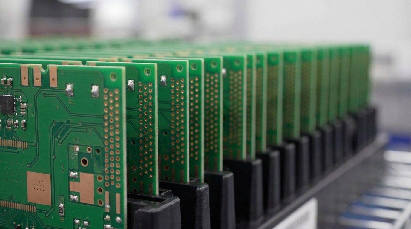
Thermal vias differ from signal vias in both function and construction. Signal vias create electrical connections between layers. Thermal vias create heat conduction paths from hot components to internal copper planes or heat sinks. This thermal role drives different design choices. Smaller via diameters support higher density arrays under component thermal pads. Filled thermal vias using conductive materials provide superior heat transfer to hollow designs by eliminating air gaps that impede conduction. Heavy copper layers then work with these thermal via arrays to form heat spreading networks in multilayer PCB stackups.
Seven Practical Best Practices for Thermal Vias
Seven focused practices improve thermal via performance in high-power PCB designs.
- Deploy dense via arrays. Place thermal vias under small to mid power QFN thermal pads, with larger arrays for higher power devices.
- Use tuned via sizing. Specify via diameters and pitch spacing for strong thermal density while preserving structural integrity and manufacturability.
- Implement filled construction. Specify copper or resin fill and capping per IPC-4761 Type VII to block solder wicking and reduce thermal resistance.
- Connect to heavy copper planes. Provide continuous solid copper connections to internal ground or power planes to minimize thermal impedance.
- Add thermal stitching. Use via stitching around hot zones to extend heat paths across multiple layers.
- Position via-in-pad strategically. Place thermal vias directly beneath exposed thermal pads of QFN and BGA packages to shorten thermal paths.
- Validate with simulation. Confirm that thermal via arrays reduce component operating temperatures through thermal modeling and analysis.
These coordinated practices create robust thermal management systems that protect high-power components from overheating while supporting efficient manufacturing.
Designing Thermal Via Array Layouts and Sizing
Grid pitch spacing sets the balance between thermal density, plating capability and anti-wicking requirements. Within these spacing limits, component thermal pad size defines the maximum number of vias that can fit. Designers then place as many thermal vias as the footprint allows without compromising mechanical structure. Final via density under component pads scales to power dissipation requirements and thermal simulation results.
To quantify thermal via performance, designers calculate thermal resistance using R = ρ × L / A, where ρ represents copper resistivity, L equals via length and A represents the cross-sectional area. Lower resistance values indicate better heat transfer and guide decisions about via diameter, count and array density. Maintaining practical aspect ratios supports void-free copper plating and structural integrity while still enabling effective heat conduction. Request a Quote for Thermal Via DFM Review to align via array configurations with specific power and reliability requirements.
Via-in-Pad and Filling Techniques for Reliable Assembly
Via-in-pad thermal designs require strict control of solder wicking during reflow assembly. Solder wicking occurs when molten solder flows into open vias during reflow and leaves insufficient pad coverage. This loss of solder coverage weakens component attachment and reduces reliability. To prevent this, designers specify filled or capped construction that blocks solder drainage while preserving the thermal conductivity of the copper barrel plating. As noted earlier, this filling eliminates air gaps that impede heat transfer and also improves mechanical stability. Manufacturing teams often tent bottom surfaces while exposing tops for heat capture, which creates flat soldering surfaces for dense BGA and QFN footprints.
Thermal Modeling and Simulation in PCB Software
Modern PCB design software supports thermal simulation of via arrays before fabrication and targets temperature differences between layers beneath heat sources. This work starts with hotspot prediction to identify problem areas around high-power components. Stackup analysis then evaluates heat spreading paths through planes and dielectric layers. Via array optimization follows and adjusts via count, placement and filling to relieve thermal bottlenecks. Design validation finally checks via current capacity and temperature rise against requirements before prototype builds. Tools such as Altium Designer and KiCad provide these thermal analysis capabilities for detailed review of via array designs.
Advanced Thermal Management for Demanding PCBs
Pro-Active Engineering provides advanced thermal solutions that extend beyond standard via arrays for extreme heat dissipation in aerospace and defense hardware. Silver sintering technology forms direct thermal paths with higher conductivity than traditional solder attachment methods. Metal-core PCB constructions integrate aluminum or copper substrates to enhance heat spreading away from hot components. Heavy copper layers increase thermal mass and current handling capacity for power-dense designs. These technologies perform well in harsh environmental conditions with wide temperature swings and vibration. Pro-Active Engineering’s ISO 9001:2015, AS9100 and ITAR certifications confirm that these solutions meet quality and security expectations for mission-critical applications.
DFM Checklist for Production Thermal Vias
Production-ready thermal via designs depend on clear manufacturing specifications. Key checklist items include via fill material selection, capping requirements for via-in-pad locations, plating thickness targets for thermal conductivity and reflow profile compatibility with assembly processes. Designers must work closely with manufacturers to determine optimal via sizes, spacing and filling options that avoid manufacturing issues. Pro-Active Engineering’s integrated design-to-production workflow addresses these factors during the design phase and reduces costly revisions while supporting a smooth transition to volume manufacturing.
Common Pitfalls in Thermal Via Implementation
Several recurring design mistakes reduce thermal via effectiveness. Poor connection to copper planes limits heat spreading capability, and insufficient via density under high-power components creates thermal bottlenecks. Unfilled vias in via-in-pad applications increase the risk of solder wicking during assembly. Inadequate aspect ratio control can cause plating voids that restrict heat transfer. Avoiding thermal reliefs on thermal vias prevents impedance to heat flow and supports direct conduction into planes. Early collaboration between design and manufacturing teams addresses these issues through clear specifications and design rule verification.
Conclusion: Building Thermally Robust High-Power PCBs
Effective thermal vias in high power PCB design rely on careful control of via sizing, array density, filling techniques and connections to heavy copper planes. These proven methods deliver meaningful temperature reductions while supporting manufacturability and assembly reliability. Pro-Active Engineering’s thermal management capabilities combine advanced via technologies with integrated design-to-production workflows to support strong heat dissipation in mission-critical applications. Request a Quote for Thermal Via DFM Review to apply this expertise to thermally efficient PCB designs for high-power electronics.
Frequently Asked Questions
How is the optimal number of thermal vias determined for a high-power component?
The optimal thermal via count depends on component power dissipation, thermal pad size and target junction temperature. Designers begin with the maximum number of vias that fit within the thermal pad footprint using recommended pitch spacing. Small to mid power QFN packages often use several vias, while larger or higher power devices require more. Thermal simulation software then validates the via array, and filled vias receive consideration when maximum thermal performance is required.
What is the difference between thermal vias and normal signal vias?
Thermal vias conduct heat rather than transmit electrical signals. They often use larger diameters, filled construction for improved thermal conductivity and direct placement under heat-generating components. Thermal vias connect to large copper planes for heat spreading across the board. Signal vias focus on impedance control and electrical performance instead of heat flow. Manufacturing specifications and design rules differ between these via types to reflect these roles.
Should designs use filled or unfilled thermal vias?
Filled thermal vias provide stronger thermal performance by eliminating air gaps and adding thermal mass, though they increase manufacturing cost. For high-power applications where thermal performance holds priority, filled vias with conductive materials deliver the strongest heat transfer. Unfilled vias can serve lower power applications or cost-sensitive designs. Via-in-pad locations almost always require filled and capped construction to prevent solder wicking during assembly.
How are thermal vias implemented in Altium Designer?
In Altium Designer, engineers create thermal vias by placing standard vias under component thermal pads and then specifying fill requirements in fabrication notes. The via stitching feature automatically generates thermal via arrays around hot regions. Vias connect to internal copper planes through solid connections instead of thermal reliefs to support heat flow. Design rules define thermal via spacing and sizing, and thermal analysis tools validate performance before fabrication.
What compliance factors affect thermal vias in defense applications?
Defense applications follow military specifications for materials, processes and documentation. Thermal via designs comply with IPC standards for workmanship and reliability, and filled materials must meet outgassing requirements for space hardware. ITAR compliance influences manufacturing location and personnel access, which drives the need for domestic production capabilities. Quality systems maintain full traceability and documentation control throughout the thermal via manufacturing process, from material sourcing through final assembly and testing.