Key Takeaways
-
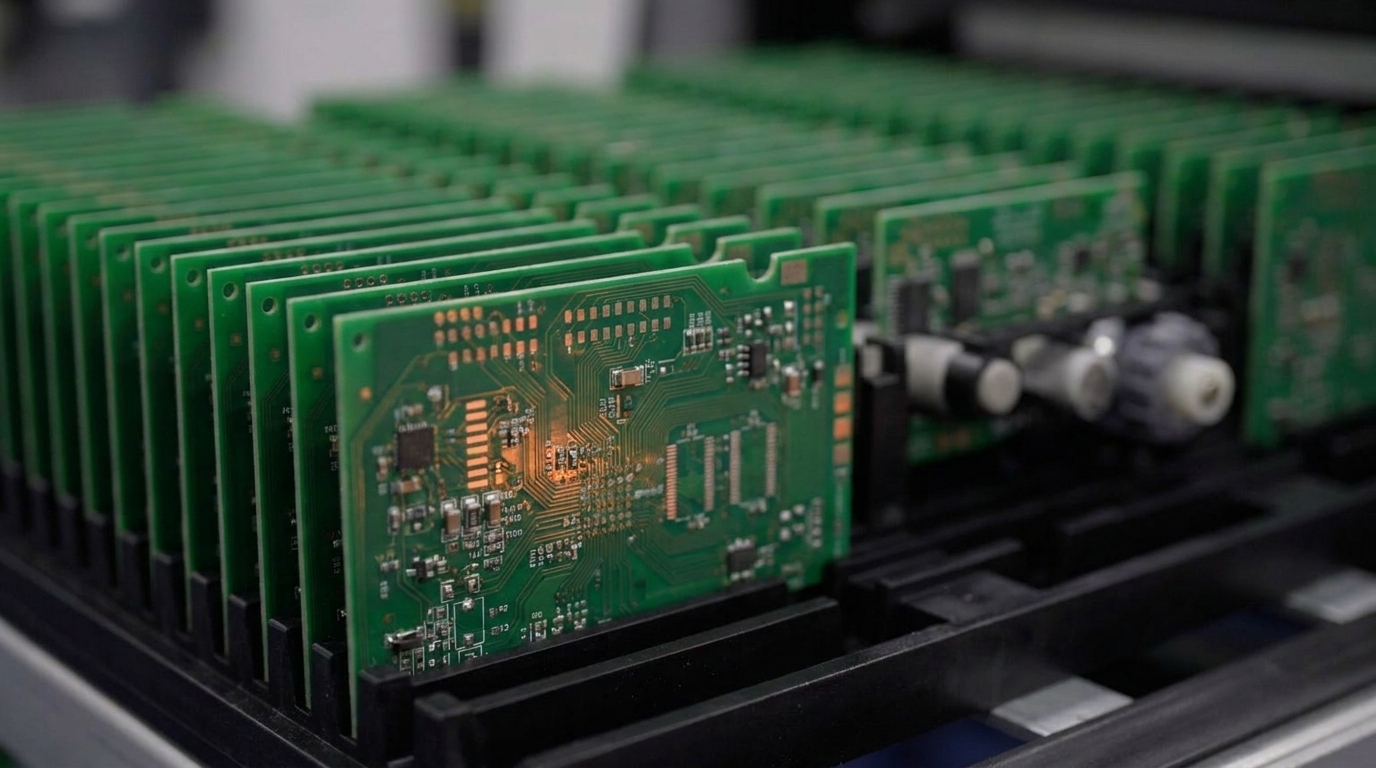
PCB thermal modeling uses CFD and FEA to predict heat distribution, identify hotspots and prevent costly redesigns in high-density electronics.
-
The seven-step simulation process, from component data gathering to physical validation, supports accurate thermal predictions and manufacturable designs.
-
Tools such as Ansys Icepak, Flotherm, Altium Designer and KiCad provide detailed analysis integrated with PCB design workflows.
-
Thermal vias, metal-core PCBs and strategic component placement increase reliability in mission-critical applications.
-
Pro-Active Engineering connects simulation and production with certified processes and advanced thermal technologies, supporting expert thermal design review.
Core Principles of PCB Thermal Modeling
PCB thermal modeling simulates three primary heat transfer mechanisms: conduction through copper traces and vias, convection to surrounding air and radiation from component surfaces. These mechanisms depend on component power dissipation, stackup configuration and via placement. Among these factors, variations in copper thickness often prove decisive and can trigger thermal runaway or temperature rise under load in high-density designs.
Thermal hotspots create cascading failures in defense and aerospace applications. These industries measure reliability using Failure In Time (FIT) rates, defined as the number of failures per billion device hours. Programs in these sectors require PCBs that maintain low FIT rates under sustained thermal stress. Via thermal resistance becomes critical in multilayer designs, where inadequate thermal paths concentrate heat and accelerate component degradation.
Traditional finite element modeling can become computationally intensive for complex thermal analysis. Recent developments address this limitation through AI-driven surrogate modeling frameworks that use finite element-based virtual design of experiments for rapid thermal-mechanical assessment. These surrogate models support efficient design refinement with reduced computational effort compared with conventional finite element modeling. The models evaluate parameters such as thermal interface material thickness, chip area and PCB layout using response surface and regression techniques.
Get a thermal design review that integrates advanced modeling with production-ready manufacturing.
Seven-Step PCB Thermal Simulation Workflow
This seven-step workflow converts thermal theory into practical simulation that supports manufacturable designs.
1. Gather Component Data: Collect power dissipation values, thermal resistance specifications and derating requirements. Strict adherence to component derating standards such as ECSS-Q-ST-30-11C keeps components below rated maximum stresses. This practice extends lifespan in space and defense applications.
2. Build 3D Model: Create accurate geometric representations that include component placement, copper layers and via structures. Import PCB layout data using industry-standard formats such as ODB++ or Gerber files.
3. Assign Materials and Boundary Conditions: Define thermal properties for substrates, copper and components. Set realistic boundary conditions, including heat transfer coefficient values for natural convection and PCB surface emissivity based on coating.
4. Mesh and Simulate: Generate a computational mesh and run CFD or FEA analysis. Increase mesh density around critical components and thermal interfaces to improve heat transfer predictions.
5. Analyze Hotspots and Gradients: Identify temperature peaks, thermal gradients and potential failure points. Compare component junction temperatures with derating requirements.
6. Optimize Layout: Adjust component placement, add thermal vias and modify copper distribution based on simulation results. Iterate design until thermal performance meets defined specifications. Once simulation results reach acceptable margins, the workflow shifts to physical confirmation.
7. Validate Physically: Verify simulation predictions using thermocouples and infrared imaging on prototypes. Calibrate models against measured data to build confidence before full production.
Common simulation platforms include Ansys Icepak for ECAD integration, Flotherm for CFD accuracy, Altium Designer for native thermal analysis and KiCad for open-source applications.
Software Platforms for PCB Thermal Analysis
Professional thermal simulation depends on software that balances accuracy with efficient design workflows. Ansys Icepak excels in ECAD import capabilities and orthotropic conductivity modeling and aligns well with design-for-manufacturability practices. The software handles complex multilayer stackups and provides detailed component-level thermal analysis suited for regulated applications.
Flotherm delivers strong CFD accuracy for complex airflow scenarios and advanced heat transfer modeling. Its strengths appear in system-level thermal analysis where convection dominates heat transfer, particularly in enclosed electronic systems.
Altium Designer provides native thermal simulation integrated directly within the PCB design environment. This integration shortens iteration cycles by flagging thermal issues during initial placement and routing.
KiCad offers open-source thermal analysis suitable for basic modeling and educational use. Although limited compared with commercial tools, KiCad supports initial design validation and early heat-spreading checks.
Pro-Active Engineering uses these tools within a single workflow that carries validated material properties and process parameters from simulation into manufacturing.
Thermal Optimization Techniques in PCB Design
Strategic component placement establishes the base for effective thermal performance. High-power components require separation from temperature-sensitive devices to prevent excessive local heat buildup. Beyond spacing, thermal via arrays beneath power components create direct conductive paths to internal copper planes and reduce thermal resistance.
When placement and via strategies reach their limits, advanced stackup materials provide additional thermal capacity. Panasonic Megtron 6 improves thermal performance while maintaining strong dimensional stability for multilayer constructions.
For applications that demand greater heat dissipation, metal core PCBs (MCPCBs) offer thermal conductivity superior to traditional FR4 materials. Aluminum cores support high thermal conductivity for moderate power levels. Copper cores provide even higher conductivity for extreme thermal loads.
Pro-Active Engineering applies exclusive thermal technologies that extend beyond standard PCB assembly. Capabilities include silver sintering for direct die attach, engineered thermal paths that bypass traditional substrate limits and heavy copper integration that reduces electrical resistance while increasing thermal mass. These methods support mission-critical thermal performance across demanding environments.
Explore advanced thermal optimization that strengthens reliability and performance.
From Simulation to Production in Thermal Design
The transition from thermal simulation to manufacturing depends on design-for-manufacturability practices that connect models with production conditions. Engineering teams align thermal simulation parameters with standards such as IPC-2152 for trace temperature rise and current-carrying capacity. This alignment helps simulated performance match manufactured boards.
Prototype validation that uses production processes reduces the gap between simulation and real hardware. Pro-Active Engineering’s Speed Shop delivers rapid prototypes built with the same materials and processes used in full production. This approach enables fast thermal validation so models can predict real-world performance before volume commitments.
Manufacturing process variables act together to shape thermal behavior. Copper thickness tolerances, via fill quality and lamination parameters all influence heat transfer characteristics. Integrated workflows include these variables in simulation models and set expectations for acceptable ranges. This coordination reduces thermal surprises during production ramp.
Case Study: A defense electronics program encountered thermal hotspots in high-power amplifier sections during initial prototyping. Pro-Active Engineering combined thermal simulation with silver sintering technology and direct thermal paths. This integrated approach delivered high reliability across wide operating ranges with full AS9100 and ITAR traceability.
Conclusion
PCB thermal modeling supports reliable high-density electronics in mission-critical applications. The seven-step simulation workflow, combined with targeted optimization techniques and production-focused validation, lowers failure rates compared with designs that lack structured thermal management.
Pro-Active Engineering provides comprehensive thermal design capabilities that connect simulation, advanced materials and certified manufacturing processes so thermal models carry through to production success. The advanced thermal technologies detailed earlier, from silver sintering to metal-core constructions, support solutions that exceed standard PCB assembly practices.
Frequently Asked Questions
What is PCB thermal modeling?
PCB thermal modeling uses simulation to predict heat distribution across printed circuit boards. The process analyzes three primary heat transfer mechanisms: conduction through copper traces and vias, convection to surrounding air and radiation from component surfaces. Engineering teams use thermal modeling to identify hotspots, refine component placement and confirm thermal performance before manufacturing. Simulations incorporate component power dissipation, material thermal properties, stackup configuration and environmental conditions to predict operating temperatures and reduce thermal failures in high-density electronics.
What is the best free PCB thermal simulation software?
KiCad provides accessible free PCB thermal simulation for basic modeling and educational work. Although less capable than commercial tools such as Ansys Icepak or Flotherm, KiCad supports fundamental thermal analysis for initial design checks and simple heat transfer calculations. The open-source platform includes basic thermal via modeling and copper plane analysis. As discussed in the simulation workflow, thermocouples and infrared imaging provide the physical validation needed to calibrate free tools. Mission-critical applications that require advanced thermal management benefit from professional simulation platforms connected with manufacturing workflows.
How do I get started with Ansys PCB thermal tutorials?
Ansys PCB thermal simulation starts with importing PCB layout data using formats such as ODB++ or Gerber files. The basic workflow creates a 3D thermal model, assigns material properties including thermal conductivity and specific heat, defines boundary conditions such as ambient temperature and convection coefficients and sets component power dissipation values. Key steps include mesh generation around critical components, steady-state or transient thermal analysis and hotspot review. Effective tutorials highlight iterative design refinement based on simulation results, with emphasis on component placement, thermal via placement and copper distribution to reach target thermal performance.
How can I avoid thermal failures in PCB design?
Preventing thermal failures relies on consistent use of the seven-step thermal simulation workflow combined with proven optimization techniques. Key strategies include strategic component placement with adequate spacing between high-power devices, thermal via arrays beneath heat-generating components, selection of stackup materials with improved thermal conductivity and use of copper planes for heat spreading. Advanced methods apply metal-core substrates for high-power designs, silver sintering for direct thermal paths and heavy copper layers for stronger current handling. Validation through prototype testing with thermocouples and infrared imaging confirms simulation accuracy before production.
What role does DFM play in thermal engineering?
Design-for-manufacturability in thermal engineering helps simulation models match production hardware while limiting redesign costs. DFM processes compare thermal designs with manufacturing constraints such as copper thickness tolerances, via fill capabilities and lamination parameters that affect heat transfer. Early DFM involvement identifies potential thermal issues during design phases rather than after tooling. Correction costs rise across later development stages, so early detection matters. Effective DFM workflows include manufacturing process variations in thermal models, specify realistic material properties based on supplier capabilities and define design rules that support consistent thermal performance across production volumes.