Key Takeaways
- Strategic component placement spreads heat, prevents hotspots and aligns with airflow patterns.
- Thermal via arrays with filled or capped vias under pads move heat efficiently into internal planes.
- Heavy copper pours, thicker copper and balanced planes increase heat spreading and current capacity.
- Metal-core PCBs, silver sintering and direct thermal paths support extreme power density designs.
- Pro-Active Engineering supports DFM-focused thermal design, rapid prototyping and simulation validation.
Design Context and Key Terms
This guide serves lead design engineers and hardware engineers who manage thermal risk in high-power, high-density boards. Key terms include thermal vias, copper pour, stackup, DFM, metal-core PCB, silver sintering and direct thermal path. The PCB market shows rising demand for thermally robust designs that support U.S. onshoring and ITAR-compliant high-reliability programs.
1. Place Components to Control Heat Flow
Component placement sets the foundation for thermal performance. Place high-power parts centrally or distribute them to avoid tight clusters that create hotspots. Maintain spacing of at least three times the component width between heat sources to prevent overlapping thermal fields. Keep temperature-sensitive parts outside these hot zones to protect performance and lifetime. Align placement with airflow so convection carries heat away from critical regions while still supporting routing density. Pro-Active Engineering’s DFM process addresses these placement decisions early in layout.
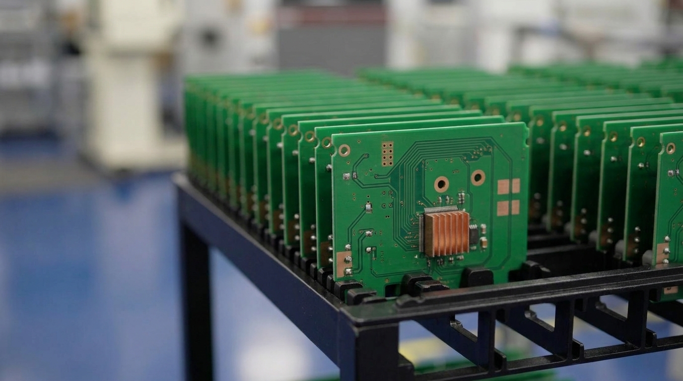
2. Build Thermal Via Arrays Under Hot Components
Thermal via arrays create vertical heat paths from component pads into internal planes. Place vias directly under thermal pads so heat moves quickly away from junctions. Thermal via diameters vary by design, with smaller vias supporting dense arrays and larger vias improving conduction per via.
PCB Thermal Via Best Practices
- Select via diameters that match power levels and available pad area.
- Use via-in-pad structures to shorten the thermal path from device to plane.
- Specify tenting, plugging or filling to control solder wicking during assembly.
- Maintain consistent spacing inside arrays to balance thermal and manufacturability needs.
- Connect thermal vias directly to internal copper planes for efficient heat spreading.
- Call out filled and capped vias where reliability and flatness matter.
Pro-Active Engineering fabricates filled and capped thermal vias with controlled plating and repeatable thermal performance.
3. Use Copper Pours and Balanced Planes for Spreading
Copper area acts as a heat spreader across the board. Maximize copper coverage with pours and solid planes around high-power regions to lower local temperatures. Use heavier copper weights where current and thermal loads demand stronger conduction. Balance copper distribution across layers to limit warpage during assembly while maintaining thermal paths. Tie thermal pads directly to large copper regions without thermal reliefs when assembly processes can support that connection.
4. Apply Thicker Copper for High Current and Heat
Thicker copper improves both current capacity and heat conduction. Use increased copper weights on power layers to move heat away from sources and reduce I²R losses. Copper’s thermal conductivity far exceeds FR-4, so copper thickness strongly influences temperature rise. Heavy copper designs support high-power converters, motor drives and similar loads. Pro-Active Engineering supports heavy copper builds with precise thickness control and consistent etching.
5. Plan Stackups with High-Tg and Thermal Planes
Stackup planning links material choice and thermal performance. Select high-Tg materials to handle elevated temperatures and reduce delamination risk. Reserve specific layers as thermal planes tied to major heat sources through via arrays. Integrate these planes during early stackup planning so signal integrity, power delivery and thermal needs align.
6. Use Metal-Core and IMS Boards for Severe Heat
Metal-core and insulated metal substrate boards handle higher thermal loads than standard FR-4. Copper-core PCBs outperform aluminum cores for conduction and support mission-critical power systems. Metal cores also improve mechanical rigidity under thermal cycling. Pro-Active Engineering offers aluminum and copper-core constructions for designs that exceed the limits of conventional laminates.
7. Run Early PCB Thermal Analysis with Free Tools
Thermal analysis guides placement, via strategy and stackup before fabrication. Run simulations early in the design phase to locate hotspots and confirm that copper and vias can carry heat away. Modern tools provide faster solvers and improved accuracy, which supports quick design iterations.
Pro-Active Engineering correlates simulation results with fabricated prototypes so models reflect real behavior. Get started with simulation validation services.
8. Reserve Space for Heatsinks and Active Cooling
Mechanical cooling hardware must fit the layout from the start. Reserve keep-out zones, mounting holes and stiff regions for heatsinks and fans during initial placement. Include thermal interface materials, gap fillers and pads in the mechanical model so heat flows cleanly from components into external cooling systems.
9. Apply the 3W Rule and Size Traces for Heat
Trace geometry affects both electrical and thermal behavior. Use the 3W rule for spacing so separation equals three times trace width, which reduces thermal and electrical coupling. Use trace width calculators to size conductors for current, temperature rise and I²R losses. Balance these calculations with copper thickness and plane support in high-current regions.
10. Move to Silver Sintering and Direct Thermal Paths When Needed
Some designs exceed the capability of standard thermal interfaces and laminates. Silver sintering technology forms low-resistance bonds that outperform many conventional thermal interface materials. Direct thermal path structures operate cooler than standard builds by removing dielectric bottlenecks under hot components. These advanced methods support compact layouts with high power dissipation while maintaining reliability targets.
11. Add Thermal Checks to DFM Reviews
DFM reviews provide a structured point to confirm thermal robustness. Integrate thermal checks into these reviews to catch issues that appear during fabrication and assembly. Balanced copper distribution reduces differential expansion during reflow, which protects solder joints and limits board warpage. Balanced copper also reduces via wicking, where solder pulls away from pads and weakens joints. Pro-Active Engineering’s DFM checklist includes validation points for these thermal and mechanical interactions from prototype through production.
12. Validate Prototypes and Align with Simulations
Prototype validation confirms that thermal models match real hardware. Use production-equivalent processes so prototype results scale to volume manufacturing. Pro-Active Engineering’s Speed Shop delivers quick-turn builds that support fast thermal test cycles. Apply infrared imaging and direct temperature measurements to compare against simulation results and refine models for final release.
Common Thermal Challenges and Fixes
Thermal via wicking during assembly can weaken solder joints and reduce reliability. Simulation and hardware mismatches often trace back to incomplete material data or oversimplified models. Pro-Active Engineering addresses these risks through engineering-led DFM reviews, full material traceability and validated modeling flows that reflect actual manufacturing conditions.
Measuring Thermal Success and Next-Level Methods
Thermal success appears in lower junction temperatures, stronger assembly yields and longer field life. Track performance with direct temperature readings, thermal images and reliability testing. Advanced simulation tools with AI-driven optimization improve prediction accuracy and shorten design cycles. Digital twin approaches support complex systems that need ongoing monitoring and refinement.
FAQ
What free PCB thermal analysis software supports design work?
Ansys provides free-tier thermal simulation for small and medium designs with professional solvers. KiCad supports open-source thermal analysis plugins for basic checks. COMSOL Multiphysics offers student versions with thermal modeling features. Many PCB layout tools now include built-in thermal estimators for early layout evaluation.
How is the thermal via count set for a design?
Thermal via count depends on power dissipation, pad size and target junction temperature. Start with simulation to estimate required heat flux through the pad. Apply via density guidelines based on power levels and available area. Confirm the final count through prototype testing and thermal measurements.
What thermal pad practices support reliable assembly?
Thermal pad reliability starts with controlled vias. Use filled and capped vias to limit solder wicking and voids. Maintain solid copper connections without thermal reliefs when assembly processes support that choice. Size pads to match component guidance while fitting the planned via array. Coordinate solder paste stencil design so solder volume supports both wetting and thermal contact.
When do metal-core PCBs outperform standard FR-4?
Metal-core substrates help when power density drives high thermal loads or when junction temperatures approach limits despite standard techniques. Aluminum cores support moderate loads and cost-sensitive designs. Copper cores serve high-power systems that need maximum thermal conductivity and strong mechanical stability.
How can thermal management align with high-speed signal integrity?
Thermal and signal goals can coexist with careful planning. Keep thermal copper features separate from high-speed routes when possible. Use dedicated thermal layers connected with vias while maintaining controlled impedance for signals. Plan stackups that support both heat spreading and signal quality, and use localized thermal zones near hot components.
Pro-Active Engineering partners with design teams to apply these thermal practices across layout, materials and manufacturing. The integrated engineering and production workflow maintains thermal performance from concept through volume build. Start a thermal-focused PCB design and prototyping project.