Key Takeaways
- Single-sided PCBs offer the lowest cost and simplest design for basic applications like LED lighting but lack signal integrity for complex circuits.
- Double-sided PCBs provide moderate density and flexibility through vias, making them ideal for automotive and industrial controls with crossed trace routing.
- Multilayer PCBs deliver strong signal integrity, EMI shielding, and thermal performance that support aerospace, defense, and high-speed applications.
- Follow the 3W rule for trace spacing and apply DFM practices like via aspect ratios to improve manufacturability and reduce redesign risk.
- Partner with Pro-Active Engineering for AS9100/ITAR-certified high-reliability PCBs with 2-5 day Speed Shop prototyping.
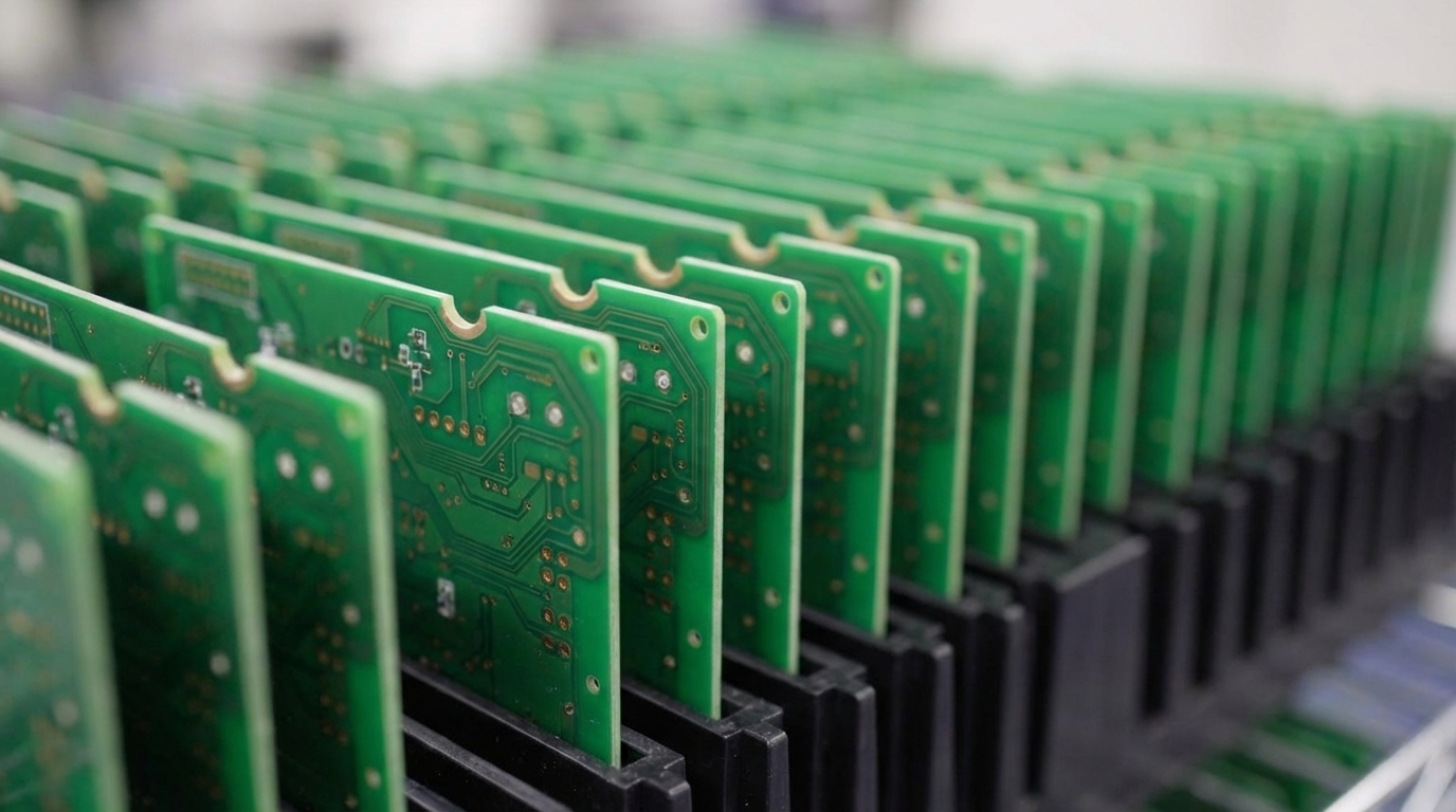
Core PCB Types and Where They Fit
The three main types of printed circuit boards are:
- Single-sided PCBs: Feature one copper layer on a single side of the substrate
- Double-sided PCBs: Contain copper layers on both sides connected through plated through-holes (vias)
- Multilayer PCBs: Stack three or more copper layers separated by insulating materials
The following table summarizes how these three PCB types compare across key design factors that influence your selection decision:
| PCB Type | Layers | Relative Cost | Complexity | Common Applications |
|---|---|---|---|---|
| Single-sided | 1 | Low | Simple | LED lighting, calculators, basic consumer electronics |
| Double-sided | 2 | Medium | Moderate | Power supplies, automotive systems, industrial controls |
| Multilayer | 3+ | High | Complex | Aerospace, defense, medical devices, high-speed computing |
Selecting the appropriate PCB type directly affects manufacturing cost, signal integrity, and long-term reliability in demanding environments. Discuss your PCB type selection with our design team to align your choice with specific application requirements and reliability targets.
Single-Sided PCBs for Simple, Cost-Sensitive Designs
Single-sided PCBs use a single copper layer bonded to one side of an insulating substrate, typically FR4 or CEM-1. Components mount on the copper side, and traces route signals without crossing paths. This straightforward construction makes single-sided boards the most economical PCB option.
Advantages:
- Lower costs from fewer materials and simplified manufacturing
- Quick turnaround times, often within two weeks
- Easy repair and troubleshooting with visible traces
- Compact, lightweight design for space-constrained applications
Disadvantages:
- Limited circuit density unsuitable for complex designs
- Poor signal integrity without dedicated ground planes
- Routing constraints that often require jump wires for crossing traces
- Inadequate heat dissipation except in metal-core variants
When designing single-sided PCBs, several technical rules help maximize their limited capabilities. Key considerations include following the 3W rule for trace spacing, which maintains center-to-center distance of at least three times the trace width to minimize crosstalk. FR4 substrates support temperatures up to 130°C while CEM-1 handles up to 110°C. Careful material selection keeps the board within safe thermal limits.
Common applications include LED lighting boards, basic calculators, simple power relays, and consumer electronics where cost control outweighs advanced performance demands.
Double-Sided PCBs: Versatility with Vias
Double-sided PCBs use copper layers on both sides of the substrate connected through plated through-holes (PTHs) or vias. This configuration doubles the available routing space while keeping manufacturing complexity and cost at a moderate level.
Advantages:
- Increased circuit density compared to single-sided designs
- Improved design flexibility that allows traces to cross on different layers
- Cost-effective for mid-range projects that balance capability and budget
- Better component placement options with top and bottom mounting
Disadvantages:
- Higher costs than single-sided boards due to the additional copper layer and via plating
- Potential via reliability issues under extreme vibration
- Limited signal integrity without dedicated power and ground planes
The 3W/3H rule applies to double-sided designs and requires spacing of three times the trace height for plane-to-plane separation to reduce interference. Because double-sided boards rely on vias to connect the two layers, via placement becomes critical for maintaining signal return paths and preventing ground loops. Poor via placement can undermine the spacing discipline established by the 3W/3H rule.
Typical applications include automotive dashboards, power converters, industrial control systems, and consumer audio equipment where moderate complexity justifies the additional cost over single-sided alternatives.
Multilayer PCBs for High-Density, High-Reliability Systems
Multilayer PCBs stack three or more copper layers separated by insulating prepreg materials, creating complex interconnect structures through various via types. These boards appear widely in automotive and industrial applications that require high reliability and compact layouts.
Advantages:
- Dedicated ground and power planes provide superior signal integrity by creating controlled impedance paths and reducing return current loops
- High circuit density that supports complex designs in compact form factors
- Enhanced EMI shielding and reduced crosstalk
- Improved thermal management through internal copper planes
- Greater mechanical strength from laminated construction
Disadvantages:
- Highest manufacturing costs and longer lead times
- Complex design requirements that demand specialized expertise
- Difficult debugging and rework of internal layer faults
- Tight manufacturing tolerances that increase yield loss potential
Multilayer PCBs typically range from 4 to 20+ layers with thicknesses from 0.4mm to 3.2mm, often using specialized materials like Rogers for high-frequency applications. Impedance control becomes critical for maintaining signal integrity in high-speed designs.
Essential applications include smartphones, aerospace avionics, medical imaging equipment, defense radar systems, and high-speed processors where performance requirements justify the additional complexity and cost.
Comparing PCB Types and Applying DFM Best Practices
Clear understanding of the trade-offs between PCB types supports design decisions that balance performance, cost, and manufacturability. Early collaboration with manufacturing partners prevents costly late-stage redesigns.
The table below compares how each PCB type performs across critical technical characteristics that affect signal quality, EMI behavior, and thermal performance:
| Characteristic | Single-sided | Double-sided | Multilayer |
|---|---|---|---|
| Signal Integrity | Poor (no ground plane) | Moderate | Excellent (dedicated planes) |
| EMI Shielding | Minimal | Limited | Superior |
| Thermal Management | Poor | Moderate | Excellent |
| Design Complexity | Simple | Moderate | High |
Key DFM practices include applying the 3W spacing rule mentioned earlier, maintaining proper via aspect ratios, and ensuring adequate copper balance to prevent warping during lamination. Pro-Active Engineering integrates DFM principles from the initial design phases, which reduces prototype iterations and accelerates time-to-market.
Advanced PCB Types for Specialized Requirements
Specialized PCB types address application requirements that extend beyond standard rigid boards. Flexible circuits continue to grow in North America, driven by automotive battery management and wearable applications.
Flexible PCBs support dynamic bending and three-dimensional routing for wearables, medical implants, and aerospace harnesses. Rigid-flex combinations provide mechanical stability in connector areas while maintaining flexibility elsewhere.
For applications where thermal management rather than flexibility is the primary concern, metal-core PCBs excel in high-power LED applications and power electronics that require strong thermal dissipation. Electric vehicles require more PCB content than conventional vehicles, which increases demand for thermally focused designs.
Pro-Active Engineering’s advanced capabilities include silver sintering and direct thermal path technologies for extreme thermal environments, supporting next-generation defense and aerospace applications. Explore advanced PCB solutions for your application with our specialized manufacturing team.
Frequently Asked Questions
What is a Type 3 PCB?
Type 3 PCB refers to multilayer boards with three or more copper layers. These designs provide superior signal integrity, EMI shielding, and routing density compared to single or double-sided alternatives. They are essential for high-speed digital applications and complex analog circuits.
How does the 3W rule apply to PCB design?
The 3W rule requires center-to-center spacing between adjacent traces of at least three times the trace width. For example, a 5-mil trace needs 15-mil spacing to minimize crosstalk. This rule applies primarily to single-sided and double-sided designs that lack dedicated ground planes.
Which PCB type is best for defense applications?
Multilayer PCBs work best for defense applications because they provide strong signal integrity, EMI shielding, and the ability to meet stringent reliability requirements. They support complex radar systems, communication equipment, and ruggedized electronics that operate in harsh environments with vibration and temperature extremes.
What are Pro-Active Engineering’s typical lead times?
Pro-Active Engineering’s Speed Shop delivers production-ready prototypes in 2-5 days using full production processes. This rapid turnaround enables quick design validation and iteration while maintaining the same quality standards as volume production runs.
How do I choose between PCB types for my application?
Selection depends on circuit complexity, signal speed requirements, environmental conditions, and cost constraints. Simple, low-frequency circuits suit single-sided designs. Moderate complexity applications benefit from double-sided boards. High-speed, high-reliability systems require multilayer construction with a carefully planned stackup.
Clear understanding of the three main PCB types and their trade-offs supports design decisions that balance performance, cost, and manufacturability. Early collaboration with experienced manufacturing partners prevents costly redesigns and supports reliable solutions for mission-critical applications. Partner with our team to leverage three decades of expertise in high-reliability PCB design and manufacturing.