Last updated: April 17, 2026
Key Takeaways
- Follow a five-step placement sequence. Start with fixed and tallest components, then heat generators, sensitive analog, decoupling capacitors, and finally small passives to avoid assembly conflicts.
- Keep component orientation and polarity consistent across the board to reduce defects and simplify automated pick-and-place programming.
- Use IPC-7351 and IPC-2221 spacing rules to prevent solder bridging and to maintain nozzle access and AOI inspection clearance.
- Place heat-generating components at least 12.7 mm from sensitive areas, and use thermal vias and edge placement to improve heat dissipation in demanding environments.
- Pro-Active Engineering’s Speed Shop delivers DFM-focused prototypes in 2 to 5 days; request a quote for reliable, production-ready PCB assemblies.
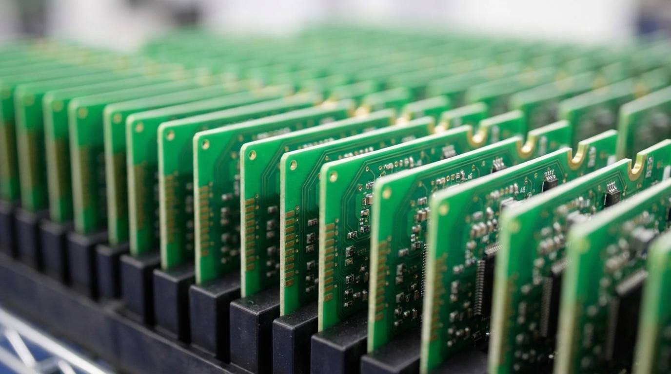
Five-Step PCB Component Placement Sequence That Reduces Rework
Following a clear placement sequence reduces rework and speeds up assembly. Start with the components that define the board’s physical limits, then move toward smaller and more flexible parts.
1. Fixed and tallest components first: Position connectors, transformers, and edge-mounted components to define board constraints and mechanical boundaries. These parts lock in keep-out zones and influence enclosure fit.
2. Heat-generating devices and thermal management: Place power semiconductors, voltage regulators, and heat sinks with enough clearance for airflow and thermal spreading. Align these parts with planned thermal vias, copper pours, or heat spreaders.
3. Sensitive analog components: Position precision references, operational amplifiers, and low-noise circuits away from switching elements and noisy digital regions. This separation reduces coupling and improves signal integrity.
4. Decoupling capacitors near integrated circuits: Place bypass capacitors within 5 mm of power pins to keep loop inductance low. Short, direct connections help stabilize supply rails during fast transients.
5. Small passive components last: Use remaining space for resistors, small capacitors, and discrete semiconductors. At this stage you can fine-tune placement for routing convenience and test access.
This sequence prevents placement conflicts and supports a smooth clockwise pick-and-place machine flow. It also shortens programming time and reduces feeder changes.
Pro-Active Engineering applies this placement sequence in our Speed Shop for prototype assemblies. Because we run prototypes through full production processes, layouts that follow this method move into volume manufacturing without major placement changes. Our engineering team extends this approach across the full system, coordinating PCB layout with firmware and mechanical design so component placement supports both manufacturability and product performance.
Component Orientation Practices That Improve Yield
Consistent component orientation improves yield and simplifies both automated and manual assembly. Aligning polarity and pin 1 markers across the board reduces placement errors and speeds inspection.
Establish a standard polarity direction for all integrated circuits and polarized components, then keep that convention across the entire design. This consistency reduces operator confusion during manual assembly and lowers programming complexity for pick-and-place equipment.
Surface-mount devices should maintain consistent orientation within each functional block, and through-hole components should share aligned insertion directions. When orientations vary, reflow heating can become uneven. One end of a component can reflow before the other end, which may cause that side to lift off the pad, a defect known as tombstoning. This risk grows when orientations differ by 90 degrees, especially for small passive components.
Clear polarity markings on the silkscreen must match the assembly documentation and the component library. These markings support quality control, rework, and field service.
Pro-Active Engineering ties orientation guidelines directly to high-speed signal routing and return path planning. This coordination keeps orientation consistent without sacrificing electrical performance. Our AS9100-certified processes include orientation checks at multiple assembly stages to catch issues early.
IPC-Based PCB Spacing Rules That Support Reliable Assembly
IPC spacing rules protect against solder defects and give assembly equipment the room it needs to work correctly. These standards also help AOI systems see critical joints and component bodies.
IPC standards establish minimum spacing requirements that support reliable assembly processes and inspection access. The following table summarizes the key IPC references that guide spacing and edge clearance for common component types, highlighting how requirements depend on component style and assembly method:
| Component Type | Min Gap (mm) | Edge Clearance (mm) | IPC Source |
|---|---|---|---|
| SMD Components | per IPC-7351 | per IPC-7351 | IPC-7351 |
| Through-Hole | per IPC-2221 | per IPC-2221 | IPC-2221 Rev C |
| High-Density SMD | per guidelines | per guidelines | Industry guidelines |
Pick-and-place equipment needs enough clearance for nozzle access and vision alignment. AOI systems require unobstructed views of solder joints and component bodies to detect bridges, opens, and misalignment. Industry guidelines for high-density layouts recommend spacing that balances compact routing with realistic assembly and inspection access.
Pro-Active Engineering uses 100% AOI and flying probe testing, so we design and build to IPC spacing standards across all assemblies. Our quality management system verifies spacing during both prototype and production builds to maintain consistent results.
Thermal Placement Strategies for Long-Life Electronics
Thoughtful thermal placement extends product life and stabilizes performance in demanding environments. Hot components need distance from sensitive circuits and a clear path to move heat away from the board.
Heat-generating components should sit at least 12.7 mm, or 0.5 inch, from temperature-sensitive devices whenever layout allows. Provide direct thermal paths from these hot spots to heat sinks, thermal vias, or copper planes to spread heat efficiently.
Power semiconductors often perform best near board edges or within defined thermal zones. These locations allow efficient heat transfer into metal-core substrates, heat spreaders, or chassis contact points. For extreme thermal challenges, advanced materials are becoming essential. Aerospace and defense sectors are adopting aerogels for thermal protection systems and advanced electronics cooling applications, showing how modern designs often combine careful placement with specialized materials.
Pro-Active Engineering’s thermal capabilities include silver sintering and direct thermal path PCB construction that move heat away from devices more efficiently than traditional interfaces. Our layouts for defense and other demanding programs pair these materials with strategic placement and metal-core designs. This combination supports high-current operation where temperature directly affects reliability and service life.
High-Density PCB Placement Tips for Mission-Critical Boards
High-density boards with 400 or more components need careful functional grouping to stay manufacturable. Grouping related circuits supports clean routing while still respecting assembly and inspection limits.
NextPCB’s February 2026 guidelines recommend placing primary BGAs near the board center for balanced routing access and reduced trace length variation. Central placement also helps manage skew and timing for high-speed interfaces.
Decoupling capacitor clusters should maintain the 5 mm power pin proximity discussed earlier, while also leaving enough space for assembly and AOI in dense areas. In defense and similar environments where these dense boards often operate, vibration resistance becomes equally important. Flexible interconnects and strain relief features need to be planned during initial placement, not added as late fixes.
HDI designs with microvias smaller than 150 microns enable escape routing from BGA pitches below 0.8 mm, which supports very compact layouts. Pro-Active Engineering’s wire bonding and flip chip capabilities extend these HDI strategies into ITAR-compliant assemblies for defense and aerospace programs.
DFM Checklist and Supporting Tools for PCB Layout
A structured DFM checklist catches manufacturability issues early and keeps projects on schedule. Use the following checks during placement reviews:
- Component placement sequence review
- IPC spacing compliance verification
- Thermal management zone planning
- Pick-and-place nozzle and feeder accessibility
- AOI and test point visibility
- Polarity and orientation consistency
- High-density routing feasibility
- Assembly fixture and panelization compatibility
- Rework and probe access planning
- Documentation completeness and revision control
Modern design tools combine DFM analysis with placement decisions. Examples include Altium Designer’s DFM extensions and SiliconExpert’s component lifecycle management. Pro-Active Engineering adds full BOM scrubbing and obsolescence risk analysis to these tools as part of our integrated design services. Request a quote for a PCB DFM best practices review to strengthen your next layout before release.
Frequently Asked Questions
How does Pro-Active Engineering ensure DFM optimization from day one?
Pro-Active Engineering builds DFM into every stage of our engineering-driven design process, from early PCB layout through firmware and mechanical integration. Our 30 years of experience with demanding programs help us spot manufacturability issues before they affect schedule or cost. The Speed Shop prototyping service uses full production processes, which keeps the transition from prototype to volume production straightforward.
What are the critical IPC spacing requirements for high-density PCB assembly?
IPC standards define baseline spacing for SMD components in standard assembly processes. High-density layouts can use tighter spacing when supported by controlled processes and capable equipment. Through-hole components need spacing that supports reliable wave soldering and manual touch-up. Typical minimum edge clearance for copper features including small through-hole components is 0.020 inches (0.51 mm), which helps prevent damage during handling and depanelization.
How does strategic component placement impact assembly yields and cycle times?
A clear placement order shortens assembly time by reducing head travel and feeder changes. Proper spacing reduces solder bridging and rework. Effective thermal placement keeps component temperatures within limits, which supports long-term reliability in demanding environments. Pro-Active Engineering’s placement strategies support high-yield prototype builds and predictable scaling into production.
What thermal management techniques are most effective for aerospace and defense PCBs?
Effective thermal management in these programs combines strategic placement with advanced materials and stackups. The silver sintering and direct thermal path technologies mentioned earlier outperform traditional interfaces by creating lower thermal resistance paths. Silver sintering can reach thermal conductivity up to ten times higher than standard thermal interface materials, and direct thermal paths remove bottlenecks created by conventional PCB stackups. Metal-core substrates and aerogel-based barriers further support extreme environments where temperature control affects mission success.
How do HDI design advancements influence component placement strategies?
High-density interconnect technologies expand placement options by enabling shorter routes and finer pitches. Microvias smaller than 150 microns and advanced stackups support via-in-pad for BGAs below 0.5 mm. Staggered microvia structures add routing flexibility while maintaining mechanical strength. These capabilities work best when design and manufacturing teams collaborate early, so placement choices remain compatible with yield targets and available processes.
Mastering PCB component placement for manufacturability depends on consistent use of proven methods, from the five-step placement sequence through thermal and DFM checks. These practices reduce redesign cycles, improve assembly yields, and support reliable performance in demanding applications. Pro-Active Engineering integrates DFM principles from concept through production to deliver assemblies that are ready for real-world conditions. Request a free DFM review and Speed Shop quote today to reduce risk on your next PCB project.