Last updated: April 17, 2026
Key Takeaways for Manufacturing-Ready Complex PCBAs
- Follow IPC-7351C land patterns, symmetric stack-ups, and defined thermal via grids to prevent warpage and yield losses in complex PCB assemblies.
- Maintain clear component spacing, board edge clearances, and asymmetric fiducials to support reliable pick-and-place and reduce solder bridging.
- Balance copper across layers and follow IPC Class 3 via and trace rules to support dense layouts that still meet high-reliability targets.
- Use structured panelization, early manufacturer collaboration, and robust test access to improve assembly efficiency, rework speed, and traceability.
- Work with Pro-Active Engineering for ITAR-certified DFM reviews and 2–5 day prototyping that reduce redesign risk before production.
Top 12 Electronics DFM Guidelines for Complex PCB Assemblies
These 12 guidelines build a practical DFM framework for complex PCB assemblies. The first group covers structural reliability, the next group focuses on placement and spacing, and the final group improves testability and collaboration. Apply them together to move from a working design to a board that builds cleanly at scale.
- IPC-7351C Land Pattern Compliance: Match every footprint to the component datasheet, including pad size, solder mask clearance, and clear pin 1 markings for automated inspection.
- Strategic Thermal Via Placement: Use 0.3 mm thermal vias in a 1.0 mm grid under power components above 1 W, and tie them to internal ground or thermal planes to create low-resistance heat paths.
- Symmetric Stack-up Design: Mirror layer pairs and balance copper density side to side so boards stay flat during reflow and through thermal cycling.
- Defined SMD Component Spacing: Keep same-type SMD parts at least one body width apart, or 0.25 mm minimum for 0402 and larger, to reduce solder bridging and rework.
- Asymmetric Fiducial Placement: Place three global fiducials at non-symmetric panel corners so pick-and-place equipment can detect orientation and correct for stretch.
- Uniform Component Orientation: Align polarized parts, such as diodes and electrolytic capacitors, in the same direction across the board to simplify programming and visual inspection.
- Defined Edge Clearances: Keep connectors and BGAs at least 1.0 mm from the board edge and smaller passives at least 0.25 mm away to reduce mechanical stress and depanelization damage.
- Via-in-Pad Management: Use filled and capped vias for via-in-pad designs, or move to advanced interconnect methods such as microvias when HDI density requires it.
- Balanced Copper Distribution: Spread copper pours and planes evenly across all layers to limit localized heating and reduce risk of bow and twist.
- Proper Panelization Gaps: Maintain 0 mm minimum spacing for V-cut separation so boards sit edge-to-edge where V-scoring is used.
- Comprehensive Test Point Coverage: Provide accessible test pads on all power rails, resets, clocks, and high-risk nets, with 0.9–1.0 mm pads and 1.3–1.5 mm pitch for reliable fixture contact.
- Early Manufacturer Collaboration: Share preliminary layouts and stack-ups with your CM before release so DFM feedback can shape the design instead of forcing late-stage changes.
Download the 2026 PCB DFM Checklist PDF and receive a complimentary manufacturability review when you submit your design for quoting.
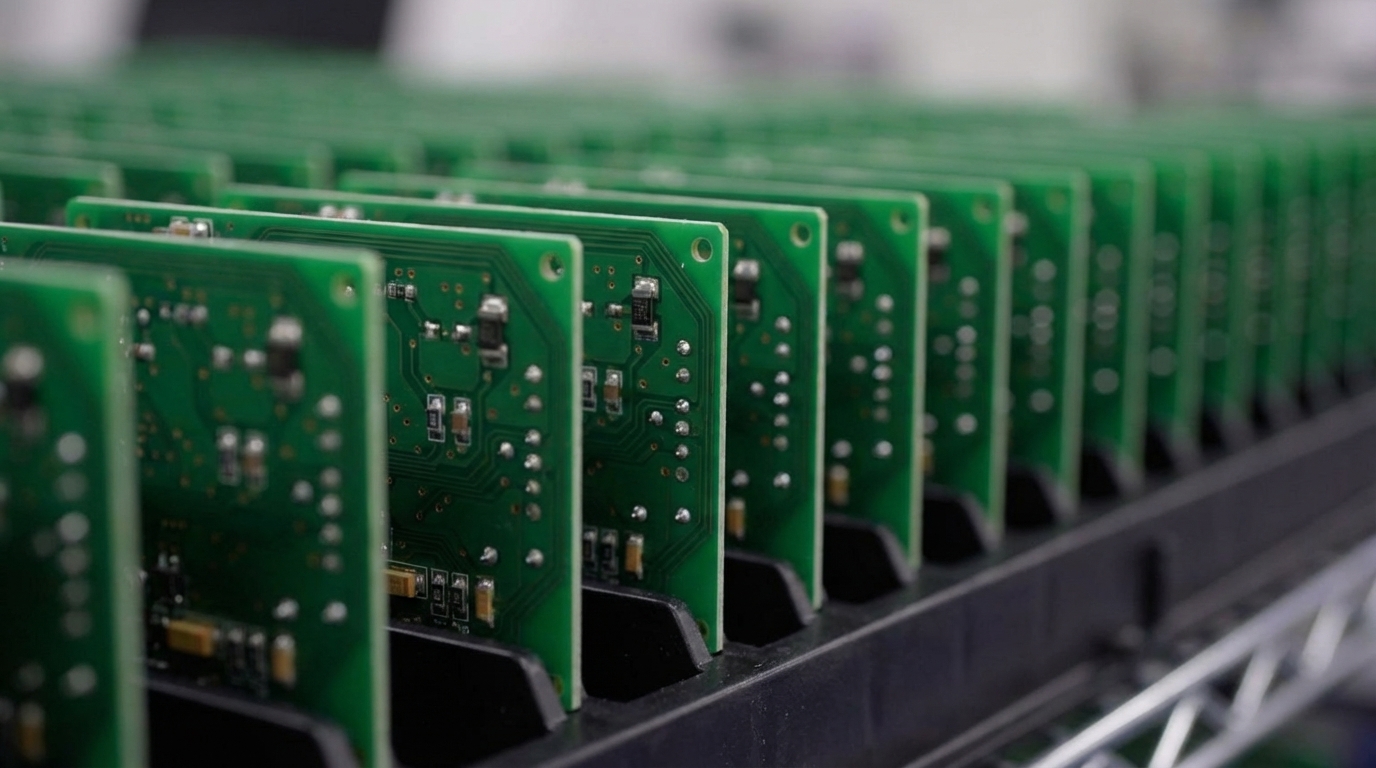
PCB DFM Checklist for Complex Assemblies
This checklist turns high-level DFM rules into concrete spacing and clearance targets that reduce solder defects and mechanical damage during assembly.
Component Spacing Requirements for SMD Packages
These minimums reduce solder bridging during reflow. Smaller packages have tighter tolerances, so spacing scales with pad geometry and paste volume.
- 01005 packages: 0.15 mm minimum spacing, roughly three times the package width, to control paste flow.
- 0201 packages: 0.20 mm minimum spacing to keep solder fillets separate under typical stencil thicknesses.
- 0402 packages: 0.25 mm minimum spacing for stable placement and consistent reflow results.
- 0603 packages: 0.30 mm minimum spacing to support automated rework and manual inspection.
- Wave soldering boards: increase spacing by at least 0.10 mm over reflow values to account for solder wave dynamics.
Board Edge Clearances for Reliable Depanelization
Edge clearances protect components from mechanical stress during handling, fixturing, and depanelization.
- Large components such as BGAs: 1.0 mm minimum clearance from the routed or scored edge.
- Standard components such as chip resistors and capacitors: 0.25 mm minimum clearance from the board edge.
- Default component body to board edge clearance is 0.25 mm unless otherwise specified, with typical values of 0.15 mm for parts smaller than 0603, 0.5 mm for connectors, canned capacitors, and crystals, and 1.0 mm for BGAs.
Pro Tip: Via-in-pad layouts need filled and capped vias or advanced flip chip processes. Pro-Active Engineering’s in-house wire bonding and flip chip assembly capabilities remove these risks through a single, coordinated process.
Component Placement and Thermal DFM Rules
Thoughtful placement supports both clean assembly and stable temperatures. Group related circuits to shorten signal paths, then keep same-type components separated enough for reliable soldering and inspection. Place power regulators with clear airflow or copper area for heat spreading, and move high-power parts toward board edges when the enclosure allows.
Thermal management becomes critical when convective cooling is limited, such as sealed or high-altitude environments. In these conditions, conductive paths carry most of the heat, so maintain clearance around high-power devices to prevent heat coupling into nearby components. Check component heights against enclosure limits early so thermal spacing does not conflict with mechanical constraints.
Common placement errors include tombstoning from uneven copper under small passives and poor thermal relief on pads tied to large planes. Pro-Active Engineering’s silver sintering technology creates direct thermal paths in aerospace applications that traditional interfaces cannot match, which reduces thermal interface failures over long service lives.
High-Density Trace, Via, and Pad Rules Aligned to IPC Standards
High-density interconnect designs rely on strict IPC rules so fabrication and assembly stay repeatable. Follow IPC-7351C land patterns and keep via aspect ratios within Class 3 limits to avoid plating issues. Minimum hole sizes down to 0.1 mm (4 mil) support via-in-pad and HDI layouts while still maintaining reliable copper plating.
The table below links three key IPC Class 3 specifications to the failure modes they control. Use it to focus design reviews on the dimensions that most often cause scrap and rework.
| IPC Class 3 Rule | Minimum Specification | Common Pitfall |
|---|---|---|
| Trace Width | Per IPC Class 3 guidelines | Bridging from insufficient spacing |
| Via Aspect Ratio | 8:1 maximum | Plating voids in deep holes |
| Annular Ring | ±0.05 mm (1.2 mil) tolerance | Breakout from misalignment |
Pro-Active Engineering’s 100% AOI and flying probe testing catch these issues before final assembly, which protects IPC Class 3 reliability in mission-critical builds.
PCB Stack-Up and Layer Management for Stable, High-Speed Boards
Symmetric stack-ups prevent warpage and support controlled impedance. This symmetry drives two key rules: place solid ground planes under high-speed traces for a stable reference, then balance copper across layers so thermal expansion forces stay even. For 12-layer designs, alternate signal and plane layers to create both the reference planes and the copper balance needed for flat, predictable boards.
Recent advances include AI-driven BOM scrubbing with tools such as SiliconExpert, which supports long-term component availability planning alongside stack-up decisions. Pro-Active Engineering’s defense case study shows how proper symmetry prevented warpage-induced failures in avionics hardware and kept flatness within spec through repeated thermal cycles.
Advanced Interconnect DFM for Wire Bonding and Flip Chip
Advanced packaging pushes density and performance, so DFM rules become tighter than in standard SMT builds. HDI designs with 0.1 mm drill capabilities enable compact routing while preserving signal integrity. For rigid-flex assemblies, keep bend radii generous and avoid sharp corners in flex regions to prevent copper cracking.
Wire bonding and flip chip assembly need precise pad sizes, surface finishes, and planarity. Pro-Active Engineering’s integrated approach combines wire bonding, flip chip, and conventional SMT in a single facility, which removes handoffs between vendors and keeps quality consistent across all interconnect types.
Panelization and Assembly Optimization to Prevent DFM Surprises
Well-planned panelization improves throughput and yield. Maintain 0 mm minimum spacing for V-cut separation so V-scored boards share a common edge, and place fiducials on panel rails for accurate vision alignment. Thoughtful panel layouts can raise material utilization from 40–50% for single boards to 80–95% for panels.
Breakaway rails should be at least 3 mm wide so clamps and conveyors can grip the panel without flexing it. Pro-Active Engineering’s high-mix, low-volume focus supports complex panel designs while still allowing smooth scaling from prototype panels to production runs.
Thermal Management DFM for Harsh Operating Conditions
Harsh environments demand aggressive thermal design to avoid early failures. Use dense thermal via arrays to move heat from sources into planes, heat spreaders, or attached sinks. Metal-core boards and silver sintering often outperform traditional thermal interface materials when current and power levels rise.
Pro-Active Engineering’s thermal expertise includes direct thermal path PCB structures and silver sintering processes that lower thermal resistance. These approaches extend product life and improve reliability in high-current and high-temperature applications.
High-Speed Signal Integrity Rules for Reliable Data Paths
High-speed signals depend on consistent impedance and clean return paths. Keep high-speed traces 10–15 mil away from board and plane edges to limit impedance shifts and EMI leakage. Match differential pair lengths within tight windows, using serpentine tuning only where needed to meet timing.
Pro-Active Engineering’s controlled impedance processes support demanding applications such as defense communications and aerospace guidance systems.
Documentation and Early Manufacturer Collaboration
Clear documentation aligned with J-STD-001 and emerging CMMC requirements supports traceability and audit readiness. Early collaboration with your manufacturer exposes DFM risks while changes remain inexpensive, which shortens development cycles and reduces scrap.
Submit your design files for a complimentary DFM review so Pro-Active Engineering’s team can highlight manufacturability limits, sourcing risks, and improvement opportunities before you lock the design.
Common DFM Issues in Complex PCB Assemblies and Practical Fixes
Complex assemblies often suffer from solder voids caused by poor thermal relief, warpage from unbalanced copper, and placement conflicts that create shadowing during reflow. These problems can cut yield by up to 20% in dense layouts.
Effective corrections include tuned thermal relief patterns, copper balancing across every layer, and early placement reviews with manufacturing input. Pro-Active Engineering’s integrated design-to-build workflow surfaces these issues while the design is still flexible, which avoids costly respins and schedule slips.
FAQ
How does early DFM collaboration reduce prototype delays?
Early DFM collaboration exposes manufacturing limits while the layout is still fluid, which prevents late redesigns that extend schedules. Pro-Active Engineering’s integrated workflow delivers production-ready prototypes in 2–5 days through the Speed Shop, using the same equipment and quality standards as full production. This continuity removes the prototype-to-production gap that many contract manufacturers struggle with.
What’s new in electronics DFM best practices for 2026?
Current DFM practice now includes AI-driven BOM analysis for obsolescence, tighter CMMC expectations for defense work, and reshoring that favors domestic capacity. Materials such as Rogers laminates for RF designs and silver sintering for thermal paths have moved into mainstream high-reliability use. Automated inspection now supports 100% checking of critical features that once relied on sampling.
Why is IPC Class 3 certification critical for complex PCBAs?
IPC Class 3 sets the reliability bar for assemblies that must operate for long periods in demanding conditions. Aerospace, defense, and medical systems often fall into this category because failures carry serious consequences. Pro-Active Engineering’s IPC Class 3 certification, combined with AS9100 and ITAR compliance, confirms that processes and documentation support these stringent requirements.
How can designers avoid DFM issues in high-reliability applications?
Designers reduce DFM risk by treating thermal paths, stack-up symmetry, and assembly clearances as primary constraints. Strategic via placement and copper balancing manage heat, while symmetric stack-ups limit warpage. Early collaboration with certified manufacturers, combined with clear test access and full-traceability documentation, keeps high-reliability projects on track.
What are the most common panelization pitfalls in complex assemblies?
Frequent panelization mistakes include cramped spacing around V-cuts, panels that flex during assembly, and fiducials that do not give clear orientation. Designers sometimes underestimate depanelization forces, which can crack solder joints or damage components. Proper panelization uses 0 mm gaps for V-cuts, well-placed support tabs, and asymmetric fiducials that machines can interpret without ambiguity.
How does Pro-Active Engineering differ from traditional contract manufacturers?
Pro-Active Engineering combines engineering, rapid prototyping, advanced assembly, and test in one coordinated workflow, which removes the communication gaps common with multi-vendor chains. Our ITAR-compliant, AS9100-certified facility brings together 30 years of experience with capabilities such as wire bonding, flip chip assembly, and silver sintering in a single location. This integrated model supports DFM-driven design from day one and smooth scaling from first article to full production.
Partner with Pro-Active Engineering for DFM-Optimized PCBAs
Complex PCB assemblies benefit from a partner who understands both design intent and manufacturing limits. Pro-Active Engineering’s 30 years of experience, 45,000 square foot facility, and 120-plus electronics specialists provide the depth needed for mission-critical work. AS9100 and ITAR certifications, combined with advanced interconnect and thermal technologies, help your designs move from concept to reliable production without unnecessary respins.
Start your DFM-focused quote to tap into Pro-Active Engineering’s integrated design-to-manufacturing process and see how 2–5 day Speed Shop prototypes can accelerate your schedule while confirming manufacturability from the first build.