Last updated: April 17, 2026
Key Takeaways
- Symmetrical stackups prevent warpage in high-reliability PCBs by balancing copper distribution across layers.
- Use the 3W spacing rule and minimum clearances to control crosstalk and support manufacturability in dense high-speed layouts.
- Strategic via placement, fiducials, and power plane design improve signal integrity, assembly accuracy, and thermal performance.
- Thermal management through trace widths, component placement, and via arrays prevents hotspots and extends component lifespan in harsh environments.
- Pro-Active Engineering’s ITAR-registered, AS9100-certified approach integrates DFM from design to production; get your free DFM review and rapid prototyping quote.
Core DFM Guidelines: 12 Precise Rules for High Reliability PCB Layouts
1. Symmetrical Stackups to Prevent Warpage
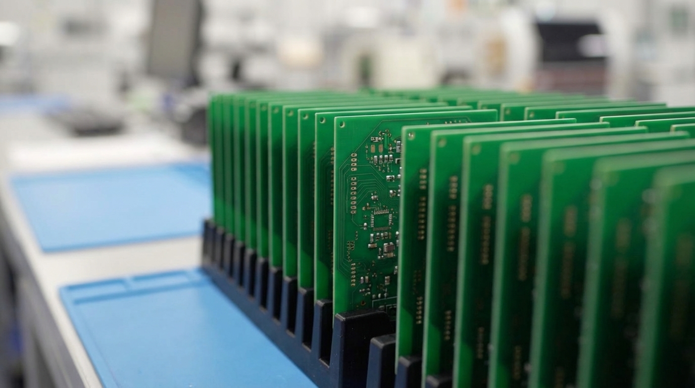
Asymmetrical copper distribution creates uneven thermal expansion that warps boards during reflow. To prevent this warpage, design stackups with balanced copper layers equidistant from the board center. In an 8-layer board, mirror layers 1–4 with layers 8–5 so copper weight stays symmetrical around the neutral axis. Even with mirrored layers, individual layers can have uneven copper coverage from traces and pads, so maintain balanced copper distribution within each layer using copper thieving or mesh patterns.
2. 3W Spacing Rule for Crosstalk Control
TONFUL Electric recommends maintaining consistent spacing between the two traces in differential pairs of typically 3–5 times the trace width for high-speed server PCB designs. Whizz Systems identifies crosstalk in AI hardware as signal interference between adjacent traces, recommending increased trace spacing and 3W rule implementation as robust signal integrity solutions. This spacing reduces electromagnetic coupling and maintains signal integrity in dense layouts.
3. Minimum Clearances for High-Rel Applications
Beyond trace-to-trace spacing, high-reliability designs must also control clearances between solder mask and pads to prevent manufacturing defects. Use 1.5–2 mil solder mask to pad clearances for fine-pitch components. Maintain 4 mil minimum solder mask web between adjacent pads. August Electronics recommends providing sufficient conveyor edge clearance around the board to allow flexibility during automated processing and prevent damage to the board or components.
4. Strategic Via Design and Stitching
Via strategy supports both signal integrity and current sharing. Place ground vias near signal vias to provide low-impedance return paths and reduce loop area. Use stitching vias every 1/10 wavelength along transmission lines to control EMI and maintain reference continuity. BestPCBs advises using multiple parallel vias at power and ground plane connections to ensure uniform current distribution.
5. Fiducial Placement for Assembly Accuracy
Accurate pick-and-place and AOI depend on clear fiducial targets. Each PCB should have a minimum of three fiducials to ensure proper placement accuracy and flexible processing, and PCBs in a panel should have three fiducials on the panel plus three on each individual PCB. Position fiducials more than 4.75 mm (0.187 inches) plus fiducial mark clearance from board edges and keep them away from tall components that could obstruct optical recognition.
6. Power Plane Design for High Current
Power planes must carry high current without creating thermal or electrical stress points. Start with 2oz or heavier copper for power planes that handle significant current so you have adequate current-carrying capacity. Within these planes, avoid narrow necks that force current into restricted paths and create current density hotspots, and ensure adequate copper area in high-current regions. In addition to plane design, BestPCBs recommends 0.3–0.5 mm diameter thermal vias directly under high-power LED pads to move heat into internal planes or heatsinks.
7. Thermal Management Through Trace Width
Trace width directly affects how much heat a PCB trace generates under load. Undersized traces create hotspots that can damage components or cause board failure. IPC-2221B uses i = 0.048 × ∆T^{0.44} × Ac^{0.725} for outer layers with 1 oz copper, while IPC-2152 is a more involved standard with over 100 charts considering factors like PCB thickness and proximity to planes. For 1 oz (35 μm) copper foil at 25°C, 10 A current requires sufficient trace width to keep temperature rise within limits. BestPCBs notes that trace width increases by about 0.4 mm for each additional 1 A for 1 oz copper.
8. Component Placement for Thermal Distribution
Component layout strongly influences local temperature rise and long-term reliability. High heat sources should be separated from electrolytic capacitors by a distance tuned within 10–30 mm under forced or natural convection to prevent lifespan reduction, which can be halved for every 10°C rise. Adjacent component bodies should maintain a minimum separation of 40 mil (1.0 mm) for assembly clearance, local thermal isolation, and safety.
9. Thermal Via Arrays for Heat Dissipation
Thermal vias create vertical heat paths that spread energy into internal planes and away from hotspots. Thermal vias under exposed pads, such as BGA or QFN, should have finished hole diameters of 0.2–0.4 mm (8–16 mil), be copper or resin filled and capped per IPC-4761 Type VII, and connect to large internal copper planes. BestPCBs recommends at least 10 thermal vias per cm² with 0.3–0.5 mm diameter beneath power devices like MOSFETs and IGBTs to form a 3D heat dissipation network.
10. Material Selection for Harsh Environments
Material choice sets the baseline for thermal, mechanical, and environmental performance. HILPCB recommends polyimide substrates for aerospace PCBs because they provide mechanical stability, high-temperature resistance, low outgassing, and radiation resistance that support durability in vibration-prone environments. BestPCBs’ material selection guide for high current PCBs suggests ceramic-filled polymers such as AlN or high-thermal-conductivity epoxy glass cloth (80–100 μm thick) to match the CTE of copper substrates (16.5 ppm/°C) and reduce thermal stress.
11. Vibration-Resistant Design Features
Vibration resistance depends on both material selection and layout details. HILPCB uses high ductility copper foil in aerospace-grade PCBs to better withstand mechanical stress from thermal cycling, which improves vibration and shock resistance. Beyond material choice, trace geometry also affects mechanical durability, so avoid 90-degree trace corners that create stress concentration points where cracks can start under vibration. Use 45-degree angles or curved transitions to distribute mechanical stress more evenly across the trace.
12. Conformal Coating Preparation
Conformal coating protects assemblies from the environment but can block access if not planned early. HILPCB applies conformal coating to all assembled aerospace PCBAs to protect against moisture, dust, corrosion, and to provide additional vibration resistance. Design test points and programming interfaces so they remain accessible after coating, using keepout areas or masking where needed.
High-Rel DFM Checklist
- Verify symmetrical stackup with balanced copper distribution.
- Confirm 3W spacing between high-speed traces.
- Check 4 mil minimum solder mask web spacing.
- Validate three fiducials minimum per board.
- Ensure adequate copper area in power regions.
- Verify thermal via arrays under high-power components.
DFM for Mission-Critical: Vibration, Thermal, Compliance & Pro-Active Integration
HILPCB conducts vibration testing for aerospace PCBs according to MIL-STD-810 Method 514.6 and shock testing according to Method 516.6 to confirm they withstand launch conditions. Mission-critical applications demand additional considerations beyond standard DFM rules.
Shock and vibration resistance requires strategic routing away from board edges and mechanical stress points. Rigid-flex PCBs enhance resistance to shock, vibration, and thermal cycling in aerospace and defense prototypes by eliminating connectors, wiring harnesses, and solder joints between boards, which reduces common failure points.
Pro-Active’s Integrated Approach
Pro-Active Engineering integrates DFM throughout the development workflow and removes the handoffs that create manufacturing surprises. Our Speed Shop delivers production-ready prototypes in 2–5 days using full production processes, which supports seamless scaling. Advanced capabilities include wire bonding, flip chip assembly, and silver sintering technology that can reduce thermal resistance compared to traditional methods.
Our quality systems include 100% AOI inspection, flying probe testing, and functional validation. ITAR registration and AS9100 certification provide secure, traceable manufacturing for defense and aerospace applications.
Experience our integrated engineering approach with a free DFM review of your next design.
Avoid These High-Rel DFM Traps & Downloadable Checklist
Common high-reliability DFM failures include:
- Late-stage thermal simulations revealing hotspots after layout completion.
- Asymmetrical stackups causing warpage during assembly.
- Insufficient fiducials creating placement accuracy issues.
- Inadequate via stitching in high-speed sections.
- Poor power plane design creating current density hotspots.
Download our comprehensive High-Reliability PCB DFM Checklist for detailed guidelines covering all critical design aspects. Download your comprehensive High-Reliability PCB DFM Checklist and schedule a consultation to review your design against these critical guidelines.
Frequently Asked Questions
What are the minimum trace clearances for high-rel PCBs?
High-reliability PCBs require 1.5–2 mil solder mask to pad clearances for fine-pitch components, with 4 mil minimum solder mask web between adjacent pads. As discussed in the 3W spacing rule above, high-speed signals need trace separation equal to three times the trace width to minimize crosstalk. Ground clearances should maintain sufficient spacing from signal traces to prevent interference.
How to calculate PCB power plane sizing?
Power plane design follows IPC standards and must provide adequate copper area in high-current regions. Use 2 oz or heavier copper for power planes that handle significant current. Refer to the IPC-2221B formula and IPC-2152 charts described earlier to relate current, temperature rise, and cross-sectional area. Use multiple parallel vias at power connections to ensure uniform current distribution.
Best fiducial rules for AOI in defense PCBs?
Defense PCBs require at least three fiducials per board for accurate automated optical inspection and component placement. Position fiducials at the minimum edge distance specified earlier, which is 4.75 mm plus clearance, to prevent damage during handling. For panelized boards, include three fiducials on the panel plus three on each individual PCB. Use 1 mm diameter fiducials with clear keepout zones free from components or traces that could interfere with optical recognition.
Vibration DFM for aerospace?
Aerospace vibration resistance requires stitching vias every 1/10 wavelength along transmission lines, polyimide substrates for mechanical stability, and conformal coating preparation for additional protection. Use high ductility copper foil to withstand thermal cycling stress. Avoid 90-degree trace corners and use 45-degree angles or curved transitions to reduce stress concentrations. Design according to MIL-STD-810 Method 514.6 for vibration and Method 516.6 for shock testing compliance.
Trace width for 10A high-rel?
For 10 A continuous current in high-reliability applications, 1 oz copper needs sufficient trace width at 25°C ambient temperature to control temperature rise. For 2 oz copper external layer at 25°C, 10 A with 10°C temperature rise requires 3.62 mm trace width. BestPCBs indicates each additional 1 A increases width by about 0.4 mm for 1 oz copper. Include design margin for critical paths and adjust for ambient temperature variations.
ITAR-compliant DFM partner?
Pro-Active Engineering provides ITAR-registered, AS9100-certified manufacturing with integrated DFM from design through production. Our Wisconsin facility offers secure, domestic manufacturing with full traceability and CMMC readiness. We integrate PCB design, rapid prototyping, assembly, and testing under one roof, which removes vendor fragmentation while maintaining strict compliance standards for defense and aerospace applications.
Boost Reliability 50%+ with Pro-Active DFM
These twelve DFM guidelines form the foundation for high-reliability PCB success in mission-critical applications. Proper implementation reduces the 30% redesign rates that plague the industry and supports first-pass assembly yields in harsh environments.
Pro-Active Engineering’s integrated approach embeds these principles from day one, combining advanced thermal management, vibration-resistant design, and rigorous quality systems. Our Speed Shop prototypes and seamless production scaling remove the disconnects that create costly surprises.
Start your mission-critical project with Pro-Active and receive a free DFM review plus 2–5 day prototyping that helps your high-reliability PCBs perform consistently from prototype through production.