Last updated: April 17, 2026
Key Takeaways
- Flip-chip PCBAs need DFT planning from the earliest design phases to reach 95%+ ICT coverage for defense and aerospace reliability.
- Use larger test pads (>1.0 mm) with wider spacing, then pair them with JTAG boundary scan to reach nets hidden under flip-chip packages.
- Combine ICT with AOI, AXI, and functional testing to approach 99%+ defect detection on high-density flip-chip assemblies.
- Select fine-pitch probes with self-cleaning tips and keep fixtures calibrated to maintain consistent, repeatable high coverage.
- Pro-Active Engineering delivers ITAR-compliant flip-chip testing with 2–5 day Speed Shop prototyping; discuss your 95%+ coverage workflow with the Pro-Active team.
Flip-Chip ICT Basics and Program Context
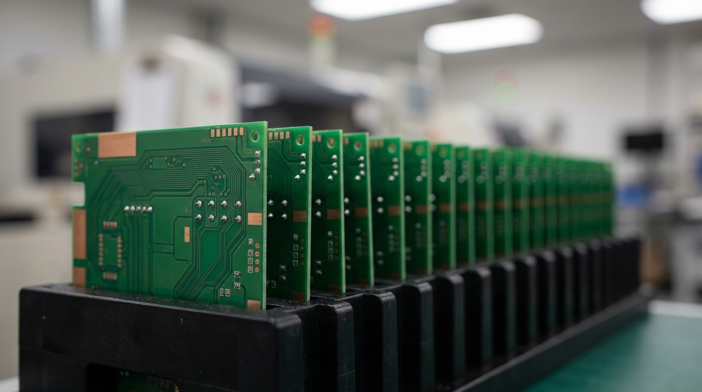
Flip-chip PCBA technology uses solder bumps directly attached to the die for electrical connection, which removes bond wires and increases I/O density compared to traditional wire-bonded packages. In-circuit testing verifies electrical connectivity and component functionality after assembly through controlled electrical measurements. Design for testability covers layout decisions, test point placement, and netlist structure that together enable thorough post-assembly verification.
The shift toward domestic manufacturing driven by ITAR requirements and supply chain security concerns increases demand for US-based partners that can handle high-mix, low-volume flip-chip assemblies. Pro-Active Engineering supports this demand with integrated engineering-to-production workflows that include PCB design, rapid prototyping through the Speed Shop with 2–5 day turnaround, advanced assembly capabilities, and comprehensive testing protocols under ISO 9001:2015, AS9100, and ITAR certifications.
Streamline your flip-chip builds with Pro-Active’s integrated design-through-test workflow.
How to Achieve 95%+ ICT Coverage: 8 Best Practices Blueprint
1. DFT Test Point Rules for Flip-Chip Accessibility
Test point specifications for flip-chip assemblies require tighter dimensional control than conventional PCBAs. Recommended test point pad sizes and spacing must match probe tip geometry and limit cross-talk during testing. Flip-chip layouts also need attention to via-in-pad designs and thermal expansion coefficients that influence probe contact reliability.
The following table compares standard PCBA test point parameters with flip-chip requirements to show how flip-chip assemblies use more conservative values to handle thermal expansion and maintain stable probe contact:
| Test Point Parameter | Standard PCBA | Flip-Chip PCBA | Rationale |
|---|---|---|---|
| Pad Diameter | >1.0 mm (40 mil), with a minimum of 0.8 mm (32 mil) for reliable probing | Typically larger | Thermal expansion tolerance |
| Spacing (center-to-center) | >1.9 mm (75 mil) preferred | Typically wider | Probe tip clearance |
| Coverage Target | >90% node access | 95%+ (as established earlier) | Mission-critical reliability |
Pro-Active Engineering’s DFM reviews apply these specifications during initial layout so test point accessibility supports the coverage goals while preserving signal integrity and thermal performance.
2. Netlist Planning and Fixture Design for High-Density Flip-Chip
High-density flip-chip layouts need fixture strategies that respect component keep-out zones and account for thermal expansion. To maintain measurement accuracy in these dense layouts, guarding techniques isolate sensitive analog circuits from digital switching noise during ICT measurements, and Kelvin probing improves resistance measurements on power distribution networks.
Beyond electrical behavior, the physical fixture must handle flip-chip package heights and thermal interface materials that influence probe access angles. Coordinated netlist planning and mechanical fixture design create a unified approach that supports stable contact, accurate measurements, and the coverage targets discussed earlier.
3. JTAG / Boundary Scan Coverage for Hidden Flip-Chip Nets
Boundary scan testing that follows IEEE 1149.1 (JTAG) protocols provides access to nets that cannot be physically probed because of flip-chip package constraints. Boundary scan testing verifies electrical connections in high-pin-count BGAs without physical probing and is particularly valuable where traditional in-circuit testing is impractical. Modern boundary scan implementations can reach more than 90% coverage of otherwise inaccessible nets within flip-chip packages.
Pro-Active’s firmware and test engineering teams handle boundary scan chain optimization and custom test vector generation that increase coverage while keeping test execution time efficient. Get a quote for JTAG-integrated flip-chip testing solutions.
4. Fine-Pitch Probing for Flip-Chip Bumps and BGAs
Feinmetall’s Fine Pitch Probes provide the precision required for challenging fine-pitch probing down to 0.11 mm in ICT and FCT applications, which helps address the dimensional constraints in flip-chip assemblies. Probe pin misalignment with fine-pitch BGA solder balls leads to poor contact, unstable connections, and unreliable test results, so specialized alignment features become essential.
Solder migration, where solder deposits in the probe tip and forms chemical compounds at high temperatures, is a common challenge in probing pads and solder bumps. Advanced probe designs use protective coatings and self-cleaning tip geometries that preserve contact reliability across thousands of test cycles.
5. Layered Testing Strategy with AOI, AXI, and Functional Test
In-circuit testing typically covers about 85% to 90% of electrical detection points on PCBs, so additional inspection methods are required to reach the coverage goals described earlier. Automated X-Ray Inspection (AXI) suits flip-chip and BGA packages on complex multilayer PCBs and detects hidden internal defects such as cold solder joints, solder voids, misalignment, and barrel defects.
Pro-Active uses a layered testing strategy that combines 100% AOI with robust ICT and targeted AXI to approach 99%+ defect detection. Thermal testing procedures then focus on flip-chip specific failure modes such as solder bump fatigue and underfill delamination, which closes remaining risk gaps that ICT alone cannot cover.
6. Fixture Maintenance and Calibration for Stable Results
Flip-chip assemblies increase ICT fixture maintenance demands because of fine-pitch probing and repeated thermal cycling. Probe tip wear monitoring and replacement schedules must reflect the higher mechanical stress of contacting solder bumps instead of traditional component leads. Calibration procedures should confirm probe contact resistance and positional accuracy across the expected operating temperature range.
Pro-Active’s Nadcap accreditation supports fixture maintenance programs that follow aerospace and defense quality expectations, with documented calibration steps that keep measurement accuracy consistent across production runs.
7. Coverage Metrics and Data-Driven Analysis
Coverage metrics for flip-chip assemblies should separate physically accessible nets, boundary scan accessible nets, and nets that require alternative verification methods. First-pass yield tracking highlights systematic issues in probe contact or thermal behavior that reduce test reliability. Statistical process control then monitors probe contact resistance trends that reveal fixture wear or contamination before failures escape.
Pro-Active’s Manex ERP system supplies real-time dashboards that track coverage metrics, test yields, and fixture performance across flip-chip production programs, which supports continuous improvement against the coverage targets defined earlier.
8. Regulated Workflow from Prototype to Production
ITAR-compliant flip-chip programs need documented testing procedures that preserve traceability from prototype through production. Pro-Active’s Speed Shop delivers production-ready prototypes in 2–5 days using the same testing protocols planned for volume manufacturing, which keeps test coverage consistent as builds scale.
Request an ITAR-compliant flip-chip test workflow review with Pro-Active’s team.
Standards, Tools, and Pro-Active Program Examples
Industry frameworks such as IPC-9252 define requirements for electrical testing of unpopulated printed boards, while JTAG boundary scan tools extend coverage verification on assembled hardware. Pro-Active’s flip-chip aerospace programs apply these standards in practice, combining silver sintering assembly processes with comprehensive electrical and thermal testing to sustain high ICT coverage and reliability.
Common Flip-Chip Test Challenges and Fixes
Key causes of probe pin misalignment with fine-pitch BGA solder balls include limitations in probe pin manufacturing and assembly accuracy, thermal expansion and elastic distortion from mechanical stress and repeated use, and equipment vibration or other external factors. Feinmetall probes provide excellent performance for solder bump probing.
Pro-Active’s flip-chip experience addresses these issues with specialized fixture designs, alignment controls, and JTAG integration that keep coverage high even when direct probing is limited.
How to Measure Flip-Chip ICT Success
Success metrics for flip-chip ICT programs include achieving the 95%+ net coverage target, holding defect escape rates below 1%, and sustaining first-pass yields above 98%. Pro-Active’s Manex traceability tools track these metrics from NPI through volume production so teams can verify performance against program requirements.
Next-Level Considerations for Advanced Programs
Emerging technologies such as AI-driven fixture optimization and digital twin modeling promise additional gains in flip-chip testing efficiency. Pro-Active’s CMMC readiness positions the company to support next-generation defense programs that require advanced cybersecurity controls alongside proven flip-chip testing capabilities.
FAQ
What ICT coverage goal should be targeted for flip-chip PCBAs?
Flip-chip PCBAs should target 95%+ ICT coverage to meet mission-critical reliability requirements. This elevated target reflects the added complexity and failure modes in flip-chip assemblies compared to conventional PCBAs that typically reach 85–90% coverage. Teams reach this higher goal through integrated DFT planning, boundary scan JTAG implementation, and complementary inspection methods including AOI and AXI.
What are the primary probing challenges with flip-chip assemblies?
Fine-pitch solder bumps create alignment challenges that can cause poor probe contact and unreliable test results. Thermal expansion differences between the PCB substrate and flip-chip package influence probe positioning accuracy during testing. Solder migration onto probe tips then degrades contact reliability over multiple test cycles. Pro-Active mitigates these challenges with specialized probe technologies, thermal management practices, and fixtures tuned for flip-chip geometries.
How does Pro-Active Engineering ensure compliance and timeline adherence?
Pro-Active maintains ITAR registration along with ISO 9001:2015, AS9100, and JCP certifications that support defense and aerospace compliance. The Speed Shop rapid prototyping service delivers production-ready prototypes in 2–5 days using the same processes planned for volume manufacturing. Integrated engineering and manufacturing workflows reduce vendor handoffs that often delay flip-chip programs.
What are the costs and benefits of integrated flip-chip testing?
Integrated testing that combines ICT, boundary scan, AOI, and AXI can reach 99%+ defect detection and significantly lower field failure costs. Per-unit testing costs may rise compared to basic ICT alone, but total cost of ownership drops through reduced rework, higher first-pass yields, and fewer field returns. Pro-Active’s end-to-end workflow also cuts vendor management overhead and shortens time-to-market.
How are flip-chip testing protocols adapted for defense applications?
Defense applications require 100% inspection with full traceability documentation. Burn-in testing simulates harsh environmental conditions to screen early failures. ITAR compliance protects sensitive designs and manufacturing data. Pro-Active’s certifications and controlled processes meet these requirements while still supporting the rapid turnaround needed for defense programs.
What thermal mitigation strategies are used in flip-chip ICT?
Thermal stress affects both the flip-chip assembly and ICT fixture accuracy during testing. Burn-in testing exposes thermal-related failures before final assembly. AXI inspection identifies thermal-induced solder joint defects including voids and cold joints. Temperature-controlled testing environments help maintain probe positioning accuracy. Pro-Active’s thermal management capabilities include silver sintering and direct thermal path technologies that improve reliability in high-temperature applications.