Last updated: April 17, 2026
Key Takeaways
- ICT delivers 85–95% fault coverage on complex PCBAs by checking resistance, capacitance, and logic through bed-of-nails or flying probe fixtures.
- Bed-of-nails supports fast parallel testing for high-volume production, while flying probe offers flexible coverage for prototypes and frequent design changes.
- An integrated test flow (AOI → Flying Probe → ICT → FCT) can reach up to 99% defect detection for mission-critical assemblies.
- DFM practices following IPC-9252 guidelines target 95% node access with proper test point spacing (>1.27 mm centers) and planned JTAG integration.
- Pro-Active Engineering delivers ITAR-compliant ICT with rapid 2–5 day prototypes; get pricing for your next project to access comprehensive testing capabilities.
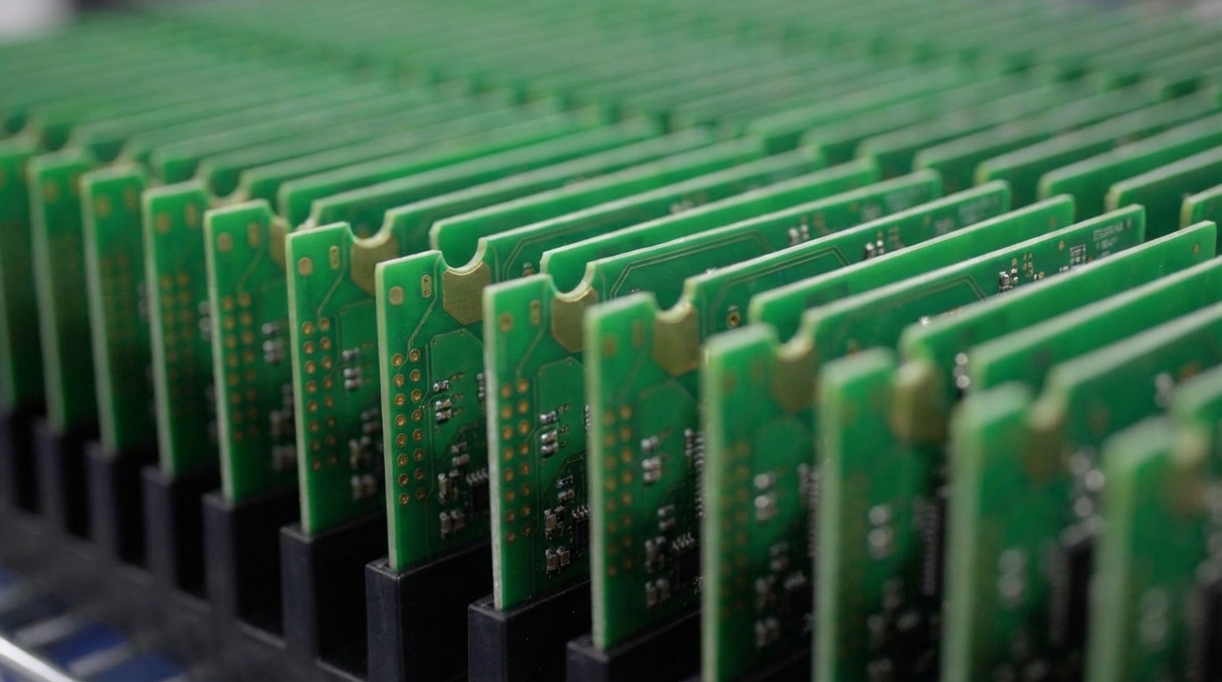
In-Circuit Testing for Complex PCBA Reliability
In-circuit testing serves as post-assembly verification before functional testing and detects manufacturing defects such as shorts, opens, missing components, incorrect values, and polarity errors. For complex PCBAs, ICT provides early fault detection that enables cost-effective rework compared to discovering issues during system-level testing.
Complex boards require specialized ICT approaches due to high component density, BGA packages with hidden solder joints, and limited probe access. Boundary-scan technology addresses limitations in probing large ICs on high-density boards by embedding test circuits within ICs to verify connections without physical probes. Guarding techniques isolate specific circuit nodes from adjacent traces to prevent false readings in densely packed layouts. The following table compares three primary testing methods and shows how ICT fits into a complete quality strategy for complex boards.
| Method | Fault Coverage | Best For Complex Boards | Speed |
|---|---|---|---|
| ICT Bed-of-Nails | 85–95% (as noted above) | High-volume production | Fast (seconds) |
| Flying Probe | Depends on accessibility | Prototypes, design changes | Slower (minutes) |
| AOI | Visual defects only | Component placement verification | Fast (seconds) |
Pro-Active Engineering’s testing stack integrates all three methods to maximize coverage while maintaining rapid turnaround times for complex defense and aerospace applications. To understand how ICT achieves this coverage, review the two primary fixture types and where each one excels.
Fixture Choices for High-Density Boards: Bed-of-Nails and Flying Probe
Bed-of-nails fixtures use arrays of spring-loaded probes that contact designated test points simultaneously, which supports very fast test cycles. These custom fixtures accommodate thousands of probes for comprehensive testing but require significant upfront investment and design time. Bed-of-nails ICT fixtures provide speed and automation for mass production of complex PCBAs but have high setup costs and limited flexibility for design changes.
Flying probe systems use movable probes that sequentially contact test points based on programmed coordinates. These testers rely on an XY mechanism with multiple probes that achieve fine-pitch access, which eliminates the need for special fixtures and suits prototypes and low-volume high-density boards. This flexibility makes flying probe ideal for prototype validation and frequent design iterations.
The table below summarizes the key tradeoffs between these two fixture types and helps you match each option to your production and design requirements.
| Fixture Type | Speed | Cost for Complex PCBA | Coverage |
|---|---|---|---|
| Bed-of-Nails | Fast (see parallel testing above) | High initial, low per-unit | 85–95% |
| Flying Probe | Slower (sequential) | Low initial, higher per-unit | Depends on accessibility |
Pro-Active Engineering maintains both fixture types in our Speed Shop, which enables optimal test strategy selection based on volume requirements and design complexity. Our engineering team evaluates each project and recommends the most cost-effective approach while maintaining comprehensive fault coverage.
The In-Circuit Test Process Step-by-Step
The ICT process starts with netlist generation from Gerber files and the bill of materials. Automated Test Program Generation (ATPG) software automatically creates ICT test programs and fixture designs from PCBA CAD data, netlists, and component libraries, significantly reducing time for complex high-node boards. Advanced 2026 implementations use AI-driven netlist generation to reduce programming time further and improve accuracy.
The testing sequence follows these steps and each step builds on the previous one.
1. Fixture Loading: The PCBA is positioned in the test fixture with probes contacting designated test points, which establishes the physical connection for all later measurements.
2. Power-Off Testing: With probes in place, the system first verifies shorts, opens, resistance, and capacitance values without applying power. This order prevents damage to components that may have assembly defects.
3. Power-On Testing: After power-off tests confirm basic electrical integrity, the system energizes the board and performs voltage measurements and basic logic verification under operating conditions.
4. Guarding Application: The tester then applies guarding to isolate specific nodes and prevent interference from adjacent circuits, which improves measurement accuracy on dense layouts.
5. JTAG/Boundary Scan: Finally, the system runs boundary-scan routines that test unprobeable areas through embedded test circuits in digital ICs.
Modern ICT systems feature adaptive probe technology that automatically accommodates different PCB types, reducing fixture replacement time. Real-time connectivity to Manufacturing Execution Systems enables immediate data upload for traceability and process optimization. While this standard process works well for many boards, high-density designs with BGAs and fine-pitch components require additional techniques.
Handling High-Density Complexity with JTAG, BGA Tools, and Fault Isolation
High-density boards present access challenges that require specialized techniques beyond basic ICT. Boundary-scan (JTAG) can supplement ICT coverage on high-density boards where traditional probing is challenging due to spatial limitations. JTAG chains enable testing of BGA interconnects and internal IC pins without physical probe access.
BGA components require indirect testing methods because solder balls sit beneath the package and remain hidden. X-ray inspection provides a non-destructive method to verify the integrity of solder joint connections in ball grid array (BGA) components on PCBAs, which lack visible leads and make visual inspection challenging. ICT complements X-ray by testing accessible peripheral circuits and power or ground connections.
Fault isolation techniques include vectorless testing, which applies AC signals through a bed-of-nails fixture and uses a sensor board pressed against the component surface to capacitively couple signals, detecting open solder joints where direct probing is challenging. This method proves particularly effective for detecting tombstoning and bridging defects on fine-pitch components.
Pro-Active Engineering’s DFM process incorporates ICT considerations from initial layout and maintains high node access through strategic test point placement and JTAG chain design. Discuss your design’s testability requirements to leverage our comprehensive fault isolation capabilities.
ICT, FCT, and Integrated Test Flow for Mission-Critical PCBA
ICT focuses on component-level verification, while Functional Circuit Testing (FCT) validates system-level performance. ICT achieves high fault coverage above 98%, suitable for early fault detection to enable rework, faster automated testing with consistent and predictable results. FCT simulates real-world operating conditions and verifies firmware execution, communication protocols, and performance under load.
The optimal test flow sequence follows AOI → Flying Probe → ICT → FCT and uses each stage for a specific role. An integrated workflow combining Automated Optical Inspection (AOI), In-Circuit Testing (ICT), and Functional Circuit Testing (FCT) can achieve up to 99% defect coverage. This integrated workflow delivers the 99% defect coverage mentioned earlier, with each stage catching different defect types and ICT providing precise fault localization for manufacturing defects.
The table below breaks down coverage type and typical metrics for each stage and shows how they complement each other across the full test flow.
| Test Stage | Coverage Type | Typical Coverage % |
|---|---|---|
| AOI | Visual/placement defects | Component placement |
| ICT | Electrical integrity | Above 98% |
| FCT | Functional performance | System-level validation |
Pro-Active Engineering implements 100% AOI inspection combined with comprehensive ICT and FCT for defense applications and delivers mission-critical reliability through layered verification.
DFM Best Practices That Improve ICT Coverage
Design for Manufacturability principles directly affect ICT effectiveness and long-term test costs. IPC-9252 guidelines target the 95% node access mentioned earlier, achieved through dedicated test points on 80%+ of nets. Key requirements include proper spacing for probe access and early JTAG chain integration.
ICT test points on PCBs should be at least 1.0 mm (40 mil) center-to-center from nearby components (preferred >1.5 mm / 60 mil), with 2 mm clearance from components under 5 mm tall. These spacing rules help probes make reliable contact without damaging adjacent components. The test points should also be evenly distributed and spaced at least 1.27 mm (50 mil) center-to-center (preferred >1.9 mm / 75 mil) to prevent probe interference during simultaneous contact. Test point diameter selection further affects probe choice, because points below 1 mm require precision probes that increase fixture costs.
Pro-Active Engineering integrates DFM considerations from initial PCB layout and plans test point placement and accessibility early. Our engineering team collaborates with customers during design review to maximize ICT coverage while maintaining signal integrity and mechanical constraints.
Conclusion: ICT as a Foundation for Reliable Complex PCBAs
In-circuit testing provides essential component-level verification for complex PCBAs and achieves high fault coverage through strategic fixture design and integrated test flow. Pro-Active Engineering’s comprehensive testing workflow, ITAR compliance, and AS9100 certification position our team as a strong partner for mission-critical applications that require rapid prototyping and reliable production scaling. Start your next mission-critical project to experience our integrated engineering and manufacturing capabilities.
FAQ
How does an ICT tester work?
ICT testers use either bed-of-nails fixtures or flying probes to make electrical contact with test points on assembled PCBAs. The system applies test signals and measures responses to verify component values, detect shorts and opens, and validate circuit integrity. Modern ICT systems include adaptive probe technology and real-time data connectivity for improved efficiency and traceability.
Flying probe vs bed of nails for complex PCBA – which is better?
Flying probe systems work best for prototypes and low-volume production because they provide flexibility and avoid custom fixture costs. Bed-of-nails fixtures provide faster testing for high-volume production but require significant upfront investment. For complex PCBAs with frequent design changes, flying probe offers better adaptability, while bed-of-nails delivers higher throughput for mature designs.
What is the difference between ICT and FCT testing?
ICT verifies manufacturing correctness by testing individual components and electrical connections without powering the full system. FCT validates design correctness by simulating real-world operating conditions and verifying system-level functionality including firmware execution and communication protocols. Both tests work together in a comprehensive quality strategy.
What is the ICT process for PCB testing?
The ICT process starts with netlist generation from design files, then proceeds through fixture loading, power-off testing for basic electrical parameters, power-on testing for logic verification, guarding application for interference prevention, and JTAG or boundary scan for unprobeable areas. Modern systems use automated test program generation to reduce setup time for complex boards.
What coverage can ICT achieve on BGA boards?
ICT coverage on BGA boards depends on test point accessibility and design-for-testability implementation. Direct BGA ball testing is impossible, but peripheral circuits, power connections, and JTAG chains enable comprehensive verification. Properly designed boards with adequate test points and boundary-scan integration can achieve 90–95% coverage when combined with complementary techniques such as X-ray inspection.