Key Takeaways
- Symmetrical MCL stackups keep warpage below 0.1% by matching copper weights and dielectric thicknesses on mirror-image layers.
- Limiting lamination cycles to fewer than 4 and using one resin system reduces via misalignment and impedance-related failures.
- Maintaining at least 2.56 mil dielectric thickness with two prepreg plies supports IPC Class 3 reliability in dense designs.
- Placing high-speed signals next to ground planes (≤5 mils spacing) and keeping via aspect ratios below 10:1 protects signal integrity.
- Pro-Active Engineering delivers DFM-compliant MCL stackups with 2-5 day prototyping; request a free quote today for mission-critical success.
MCL Stackup Symmetry Rules for Reliable Fabrication
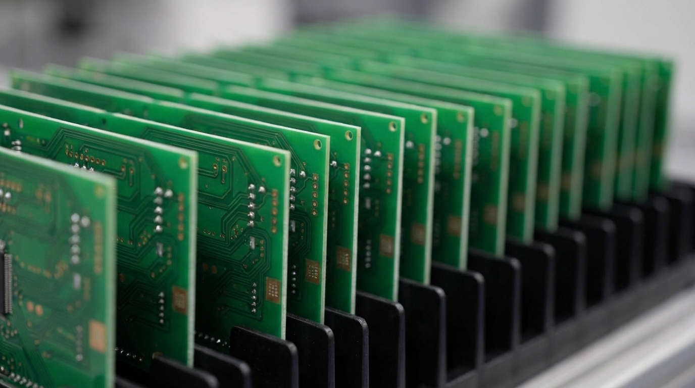
Successful MCL stackup design follows clear symmetry rules that reduce mechanical stress and improve manufacturing reliability. Symmetrical stackup prevents warping during manufacturing by balancing copper and dielectric distribution, reducing stress during lamination and soldering.
The core DFM rules for MCL layer stackups include the following guidelines.
1. Symmetry Requirements: Maintain mirror symmetry above and below the board center with identical copper foil types and thicknesses for corresponding layers. Target warpage below 0.1% by ensuring L2 and L5 have the same copper weight and routing density in 6-layer designs.
2. Material Consistency: Use one resin system throughout the stackup to prevent differential expansion. Avoid hybrid constructions that mix different dielectric materials within the same lamination cycle.
3. Lamination Cycle Limits: Keep lamination cycles below 4 to control layer registration and dimensional stability. Each additional cycle raises the risk of via misalignment and impedance variation.
4. Minimum Dielectric Thickness: For IPC Class 3 boards, maintain dielectric thickness of at least 2.56 mil using two prepreg plies. This thickness supports insulation margins and reduces the chance of electrical failure.
5. Reference Plane Placement: Place high-speed signal layers next to solid ground planes with spacing ≤5 mils (0.127 mm). This structure improves impedance control and lowers EMI.
6. Copper Distribution Balance: Distribute mechanical stress evenly by using identical core thickness, copper weights, prepreg type, and dielectric thickness on both sides of the center plane.
|
Aspect |
MCL Tolerance |
Pro-Active DFM Tip |
|
Dielectric Thickness |
±10% |
Use symmetric pairing to reduce stress |
|
Layer Registration |
±2-3 mils |
Limit lamination cycles for control |
|
Warpage Target |
<0.1% |
Balance copper across the stack |
Preventing MCL Stackup Warpage and Common Pitfalls
Preventing bowing in 12+ layer stackups starts with managing copper density differences between layers. Symmetric stackups improve flatness and stability while reducing process complexity and scrap risk compared to asymmetric designs.
Unbalanced routing density between matching layers creates differential stress during thermal cycling and often drives warpage. Excessive lamination cycles or poor registration control during sequential lamination increase the chance of via misalignment and related defects.
Pro-Active Engineering uses an integrated approach that addresses these issues through early DFM collaboration and controlled manufacturing processes. Get your MCL stackup reviewed by our DFM experts to avoid costly late-stage corrections.
Advanced MCL Construction and Via Design Rules
Foil construction with prepreg is preferred by modern fabricators as it is easier than full-core builds, especially for HDI applications that use sequential lamination. This construction method improves dimensional control and supports tighter via tolerances.
For high-density interconnect (HDI) stackups, keep aspect ratios below 10:1 to support reliable via plating. Aspect ratio below 10:1 ensures plating uniformity and prevents connectivity issues from drill shift or poor registration control.
Via placement should maintain at least 15 mil spacing to prevent overlapping antipads that disturb return paths in high-speed designs. Arrange vias in grid patterns and preserve symmetry for differential pairs to maintain signal integrity.
MCL Panelization and Alignment Control Practices
Robust panelization reduces fabrication defects and keeps hole alignment consistent across the panel. Minimum spacing of 0.5 mm (20 mils) between NPTH edges prevents structural weaknesses during panel separation.
Accurate alignment control depends on well-placed fiducial marks and tooling holes. Use alignment holes (fiducial marks) to support accurate layer registration and reduce misalignment during multi-step lamination.
Key panelization specifications include NPTH positional tolerance of ±0.05 mm (2 mils) and finished hole diameter tolerance of ±0.08 mm for CNC drilling. These tolerances become more critical as layer counts move beyond 12 layers.
Why Pro-Active Engineering Excels at MCL Stackups
Pro-Active Engineering applies 30 years of experience to mission-critical PCB applications. Our ITAR-compliant, AS9100-certified facility supports advanced interconnect technologies such as wire bonding, flip chip assembly, and silver sintering for direct thermal path designs.
Our Speed Shop delivers production-ready prototypes in 2-5 days using the same processes as full-scale production, rather than splitting design and manufacturing across vendors. This approach removes the prototype-to-production disconnect that often slows traditional contract manufacturers.
Customers such as Leonardo DRS and Vortex Optics depend on our integrated workflow for complex PCBs in defense and aerospace programs. Our engineering-driven process builds DFM compliance into the design from day one, which lowers total program risk and shortens time-to-market.
Partner with Pro-Active Engineering for your next MCL stackup project and see the impact of true design and manufacturing integration.
FAQ
What are the maximum lamination cycles recommended for MCL stackups?
MCL stackups should be limited to fewer than 4 lamination cycles to prevent layer misregistration and maintain dimensional stability. Each additional cycle increases the risk of via misalignment and impedance variations that can cause electrical failures in mission-critical applications.
What are the IPC Class 3 prepreg requirements for MCL stackups?
IPC Class 3 applications require minimum dielectric thickness of 2.56 mils using at least two prepreg plies. This structure provides insulation between layers and helps prevent electrical breakdown under high-reliability operating conditions typical in aerospace and defense applications.
How does Pro-Active Engineering ensure MCL DFM compliance?
Pro-Active Engineering integrates DFM review into the initial design phase through our engineering-driven workflow. Our team evaluates stackup symmetry, material selection, via configurations, and thermal management requirements before fabrication begins. This approach removes many redesign cycles and supports first-pass success.
What is the minimum dielectric thickness for MCL stackups?
Minimum dielectric thickness varies by application, but IPC Class 3 requires at least 2.56 mils with two prepreg plies. High-frequency applications may use thicker dielectrics for impedance control, while thermal management designs can benefit from thinner dielectrics with direct thermal paths.
What are the best MCL stackup symmetry rules?
Optimal MCL symmetry uses mirror-image construction above and below the board center, with identical copper weights, core thicknesses, and prepreg types on corresponding layers. Maintain copper density balance within ±10% between symmetric layers and target overall warpage below 0.1% for high-reliability applications.
What panelization guidelines apply to MCL stackups?
MCL panelization uses minimum 0.5 mm spacing between non-plated through holes, ±0.05 mm positional tolerance for alignment features, and strategic fiducial placement for layer registration control. V-score spacing and tab design should account for the higher rigidity of high-layer-count constructions.
Conclusion: Building Reliable MCL Stackups from Day One
Successful MCL stackup design follows strict symmetry rules, consistent materials, and controlled lamination cycle limits. These DFM guidelines reduce warpage, misalignment, and impedance failures that often affect mission-critical prototypes in defense and aerospace programs.
Request a free DFM review for your MCL stackup at Pro-Active Engineering and access 2-5 day prototypes with mission-critical reliability. Our integrated engineering and manufacturing workflow supports first-pass success and a smooth transition to production.