Last updated: April 17, 2026
Key Takeaways
- High-density PCBs exceeding 50W/cm² need coordinated passive strategies like thermal vias, copper coins, and heavy copper planes to control hotspots and avoid failures.
- Silver sintering and direct thermal path technology deliver measurable heat dissipation gains with thermal conductivities over 200 W/m·K, clearly outperforming traditional soldering.
- DFM principles applied from simulation through prototype prevent costly redesigns, and Pro-Active Engineering’s Speed Shop supports 2-5 day turnaround with 1-piece minimums.
- ITAR-compliant, US-based manufacturing with AS9100 certification protects defense and aerospace programs while maintaining mission-critical reliability.
- Pro-Active Engineering delivers proven thermal solutions; get a quote for your high-density PCB project.
Thermal Hotspots in High-Density Mission-Critical PCBs
Mission-critical PCBs in defense and aerospace must survive extreme environments and still perform reliably. Thermal hotspots form when heat generation exceeds the board’s ability to dissipate it. Localized temperature spikes then drive component degradation, solder joint fatigue, and system failures during vibration or temperature cycling.
The High Tg FR-4 variants in the FR-4 Copper Clad Laminated Sheet market are projected to grow at a 4.8% CAGR as designers demand higher thermal resistance in compact electronics. This trend shows how often traditional materials fall short in high-power layouts.
Even with better materials, accurate thermal performance still depends on detailed analysis. Thermal simulation tools like Altium Designer and computational fluid dynamics (CFD) software predict hotspot formation, yet simulation-to-fabrication gaps appear when manufacturability constraints are not considered early. IPC-6012 rigid PCB performance standards include thermal cycling tests that define baseline expectations for mission-critical hardware.
Common DFM pitfalls in thermal design include poor via placement, limited copper area for heat spreading, and material choices that ignore manufacturing tolerances. These issues compound in dense layouts where tight spacing restricts traditional cooling options.
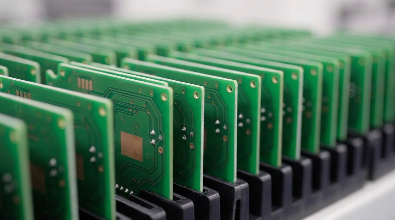
Passive Cooling That Works: Vias, Copper Coins, and Heavy Copper Planes
Passive thermal techniques create the base layer of effective heat dissipation in high-density PCBs. Designers gain the best results when they align these strategies with real manufacturing capabilities.
Thermal Vias PCB Implementation: Thermal vias beneath power devices create direct heat paths from component pads into internal copper planes. Via-in-pad configurations improve thermal coupling, and they require controlled manufacturing to prevent solder wicking. Well-designed thermal via arrays can cut thermal resistance far more than solid copper pads alone.
Copper Coins for PCB Thermal Enhancement: Embedded copper coins or slugs add local thermal mass and improve heat spreading under high-power components. These thick copper features, typically 0.5-2.0 mm, create low-resistance heat paths that noticeably improve junction temperatures. Manufacturing success depends on precise registration and specialized lamination that prevents delamination around the coin interface.
Heavy Copper Planes: High-thermal-conductivity substrates such as aluminum-core substrates with thermal conductivity of 150-235 W/m·K or specialty or modified FR-4 with thermally conductive fillers or modified resins that can have thermal conductivity of 2.2 to 3.2 W/m·K combined with heavy copper layers from 3 to 10 oz provide strong heat spreading. Pro-Active Engineering’s direct thermal path approach uses these materials to reduce thermal bottlenecks while still protecting signal integrity.
When to Move Beyond Passive Cooling in PCB Designs
Microfluidic and Active Cooling Integration
Designers move to advanced cooling once power density and temperature targets exceed what passive techniques can handle. When power densities climb beyond roughly 50W/cm² or passive methods cannot keep junction temperatures below about 85°C, active cooling becomes necessary. Direct-to-chip cooling integrates seamlessly into legacy infrastructure with superior thermal performance and can reduce temperatures by 20-30°C in demanding applications.
Embedded heat pipes inside PCB structures provide very high effective thermal conductivity through phase-change heat transfer. AI server applications in 2026 increasingly rely on these techniques as power densities continue to rise and passive approaches alone cannot maintain safe operating margins.
Liquid Cooling Trends and Performance
These PCB-level thermal challenges mirror broader trends in data center infrastructure. The data center industry’s move toward higher power densities drives rapid liquid cooling adoption. High-density data centers have current 100–132 kW AI/GPU-intensive systems per rack, and next-generation systems will exceed those values. Immersion liquid cooling supports 50-250 kW per rack with PUE of 1.05-1.15, which shows clear efficiency gains over traditional air cooling.
Silver Sintering and Direct Thermal Paths in PCB Thermal Management
Pro-Active Engineering focuses on attachment and board technologies that outperform conventional solder joints. Silver sintering achieves very low junction-to-case thermal resistance for GaN HEMTs and similar devices, which highlights its strong thermal performance.
Silver sintering AccuLam achieve thermal conductivities exceeding 200 W/m·K, approaching that of bulk silver and far surpassing traditional lead-free solders and conductive epoxies. This performance can reduce thermal resistance by about 40% compared to common attachment methods.
Direct thermal path PCB technology removes the PCB substrate from the main heat path so components transfer heat straight into external cooling hardware. These aluminum-core substrates, noted earlier for their 150-235 W/m·K conductivity, act as efficient heat highways that bypass typical PCB thermal bottlenecks.
DFM Checklist for Thermal PCBs: From Layout Decisions to Prototypes
Effective thermal management starts with Design for Manufacturability at project kickoff. Start with component placement and position heat-generating devices to maximize thermal coupling with available heat sinks, since placement drives every downstream choice. Once placement is stable, adjust the stackup to create copper distribution that supports both routing needs and the thermal conduction paths defined during placement.
Low junction-to-ambient thermal resistance targets for high-power components, validated with thermal simulation tools, give a clear metric for design success. However, meeting those targets in production requires avoiding DFM issues such as poor via fill that creates thermal barriers and copper thickness that falls short in key heat paths.
Pro-Active Engineering’s DFM-integrated workflow addresses these pitfalls from the first design review. The Speed Shop supports 2-5 day prototype delivery with 1-piece minimum order quantities, which allows rapid thermal validation before committing to production tooling. Start your DFM review and use this integrated design-to-manufacturing process for your thermal management needs.
ITAR-Compliant Thermal Management for Defense and Aerospace
Defense and aerospace programs need strong thermal performance and strict security compliance. Pro-Active Engineering maintains ITAR registration, AS9100 certification, and Nadcap accreditation to support classified and export-controlled work.
Standards such as IPC-6012 for rigid PCB performance and UL 94 V-0 for flammability guide aerospace designs, while additional testing verifies performance under vibration, shock, and temperature cycling. Automated Optical Inspection (AOI) and functional testing maintain full traceability throughout manufacturing.
US-based production removes supply chain risks tied to offshore manufacturing and still delivers advanced thermal capabilities. This domestic model supports program security and fast response times that overseas options rarely match.
Aerospace Case Study: Lowering PCB Temperatures in a Sealed Enclosure
An aerospace customer needed thermal control for a high-density PCB inside a sealed enclosure with very limited airflow. The original design used conventional thermal vias and standard FR-4 and showed hotspots above 85°C during qualification.
Pro-Active Engineering redesigned the thermal stack using silver sintering die attach and direct thermal path technology, which cut peak operating temperatures by about 30%. The new architecture added embedded copper coins under critical components and optimized via arrays tied into aluminum-core heat spreading layers. This combined approach removed thermal failures and preserved the compact form factor required for the platform.
The project highlighted the value of tightly linked engineering and manufacturing. Thermal validation finished during the prototype phase, and the design moved smoothly into production quantities. Explore similar thermal solutions for your mission-critical applications.
Frequently Asked Questions
What are the best PCB materials for thermal conductivity in high-density applications?
High-Tg FR-4 variants improve thermal performance over standard FR-4 and provide glass transition temperatures of 170°C or higher for better reliability at elevated temperatures. Metal-core substrates reach thermal conductivities above 200 W/mK, which suits power electronics and LED systems. Aluminum-core and copper-core materials offer the strongest thermal performance, while modified FR-4 blends balance thermal behavior with cost. Pro-Active Engineering tailors material selection to each project’s thermal targets, electrical limits, and manufacturing needs.
What are thermal vias PCB best practices for maximum effectiveness?
Effective thermal via design places vias directly beneath power components. Via-in-pad layouts provide strong thermal coupling and require controlled processes to avoid solder wicking during assembly. Thermal vias should connect straight to internal copper planes or heat spreading layers, and via fill processes must create continuous thermal paths. Proper implementation can significantly reduce thermal resistance compared to solid copper pads.
What are the main challenges in liquid cooling PCB design?
Liquid cooling design must address material compatibility to avoid corrosion, seal integrity to prevent leaks, and long-term reliability under thermal cycling. Coolant selection needs to balance thermal performance, electrical safety, and stability over time. Hybrid air-liquid systems often provide a practical path by cooling only high-power components with liquid and using air for lower-power devices. These hybrid designs can deliver 20-40% energy savings compared to air-only cooling while maintaining reliability.
What are the key benefits of silver sintering thermal management?
Silver sintering delivers thermal conductivities above 200 W/mK and clearly outperforms typical solder joints. The process creates very low junction-to-case thermal resistance, which improves heat extraction from high-power semiconductors. Silver sintering also improves reliability during thermal cycling and supports thinner bond lines that further reduce thermal resistance. Wide-bandgap devices such as SiC and GaN benefit strongly from this attachment method at high power densities.
How can I ensure ITAR-compliant high density PCB thermal solutions?
ITAR-compliant solutions require US-based manufacturing, proper security clearances, and controlled facility access. Pro-Active Engineering maintains ITAR registration along with AS9100 and Nadcap certifications to support defense and aerospace programs. All thermal management work, from design through production, occurs in secure domestic facilities with full traceability and documentation control. This structure protects program data while delivering advanced thermal performance.
What are typical prototype lead times for thermal PCBs?
Pro-Active Engineering’s Speed Shop delivers thermal prototypes in 2-5 days with 1-piece minimum orders. This fast turnaround uses full production processes so prototype thermal results closely match production behavior. The integrated design-to-manufacturing workflow removes common prototype-to-production mismatches that affect thermal performance. Rapid prototypes support iterative thermal refinement before you commit to tooling and volume builds.
Conclusion: Secure Reliability with Pro-Active Engineering
Advanced thermal management for high-density mission-critical PCBs depends on integrated engineering that combines proven passive methods, modern active cooling, and experienced manufacturing. Pro-Active Engineering’s blueprint delivers the thermal performance gains described throughout this article, from copper coins and heavy copper planes to silver sintering and direct thermal paths, while maintaining ITAR compliance and rapid prototype support.
Get your comprehensive DFM review and ITAR-compliant thermal PCB solutions that support mission success in demanding environments.